Datasheet 搜索 > AC-DC转换器 > Infineon(英飞凌) > ICE2A765P 数据手册 > ICE2A765P 数据手册 11/36 页

¥ 12.054
ICE2A765P 数据手册 - Infineon(英飞凌)
制造商:
Infineon(英飞凌)
分类:
AC-DC转换器
封装:
TO-220-6
Pictures:
3D模型
符号图
焊盘图
引脚图
产品图
页面导航:
引脚图在P6P7P8Hot
典型应用电路图在P3
原理图在P9
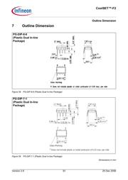
封装尺寸在P33P34P35
焊盘布局在P32
标记信息在P33
功能描述在P10P11P12P13P14P15P16
技术参数、封装参数在P17
电气规格在P16P17P18P19P20P21P22P23P24P25P26P27


导航目录
ICE2A765P数据手册
Page:
of 36 Go
若手册格式错乱,请下载阅览PDF原文件
Version 2.6 11 25 Dec 2006
CoolSET™-F2
Functional Description
secondary output voltage is insensitive on line
variations. Line variation changes the current
waveform slope which controls the duty cycle.
The external R
Sense
allows an individual adjustment of
the maximum source current of the integrated
CoolMOS™.
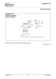
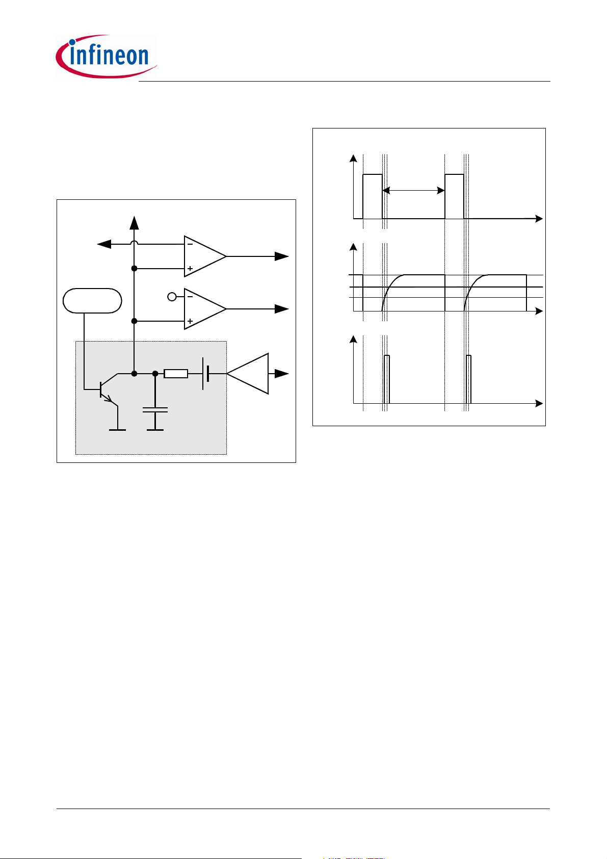
Figure 9 Improved Current Mode
To improve the Current Mode during light load
conditions the amplified current ramp of the PWM-OP
is superimposed on a voltage ramp, which is built by
the switch T
2
, the voltage source V
1
and the 1st order
low pass filter composed of R
1
and C
1
(see Figure 9,
Figure 10). Every time the oscillator shuts down for
max. duty cycle limitation the switch T2 is closed by
V
OSC
. When the oscillator triggers the Gate Driver T2 is
opened so that the voltage ramp can start.
In case of light load the amplified current ramp is to
small to ensure a stable regulation. In that case the
Voltage Ramp is a well defined signal for the
comparison with the FB-signal. The duty cycle is then
controlled by the slope of the Voltage Ramp.
By means of the Comparator C5, the Gate Driver is
switched-off until the voltage ramp exceeds 0.3V. It
allows the duty cycle to be reduced continuously till 0%
by decreasing V
FB
below that threshold.
Figure 10 Light Load Conditions
3.2.1 PWM-OP
The input of the PWM-OP is applied over the internal
leading edge blanking to the external sense resistor
R
Sense
connected to pin Isense. R
Sense
converts the
source current into a sense voltage. The sense voltage
is amplified with a gain of 3.65 by PWM OP. The output
of the PWM-OP is connected to the voltage source V1.
The voltage ramp with the superimposed amplified
current signal is fed into the positive inputs of the PWM-
Comparator, C5 and the Soft-Start-Comparator.
3.2.2 PWM-Comparator
The PWM-Comparator compares the sensed current
signal of the integrated CoolMOS
TM
with the feedback
signal V
FB
(see Figure 11). V
FB
is created by an
external optocoupler or external transistor in
combination with the internal pull-up resistor R
FB
and
provides the load information of the feedback circuitry.
When the amplified current signal of the integrated
CoolMOS™ exceeds the signal V
FB
the PWM-
Comparator switches off the Gate Driver.
x3.65
PWM OP
0.8V
10k
Ω
Oscillator
PWM Comparator
20pF
T
2
R
1
C
1
FB
PWM-Latch
V
1
C5
0.3V
Gate Driver
Voltage Ramp
V
OSC
Soft-Start Comparator
t
t
V
OSC
0.8V
FB
t
max.
Duty Cycle
0.3V
Gate Driver
Voltage Ramp
器件 Datasheet 文档搜索
AiEMA 数据库涵盖高达 72,405,303 个元件的数据手册,每天更新 5,000 多个 PDF 文件
