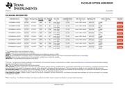
Datasheet 搜索 > National Semiconductor(美国国家半导体) > LM25088QMH-1 数据手册 > LM25088QMH-1 数据手册 10/39 页

¥ 0
LM25088QMH-1 数据手册 - National Semiconductor(美国国家半导体)
制造商:
National Semiconductor(美国国家半导体)
Pictures:
3D模型
符号图
焊盘图
引脚图
产品图
页面导航:
引脚图在P3P4Hot
典型应用电路图在P1P8P20P29
原理图在P1P10P20P30P31
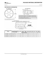
封装尺寸在P34P36P37
标记信息在P34P35
封装信息在P33P34P35P36P37
技术参数、封装参数在P5
应用领域在P1P39
电气规格在P5P6P7
导航目录
LM25088QMH-1数据手册
Page:
of 39 Go
若手册格式错乱,请下载阅览PDF原文件
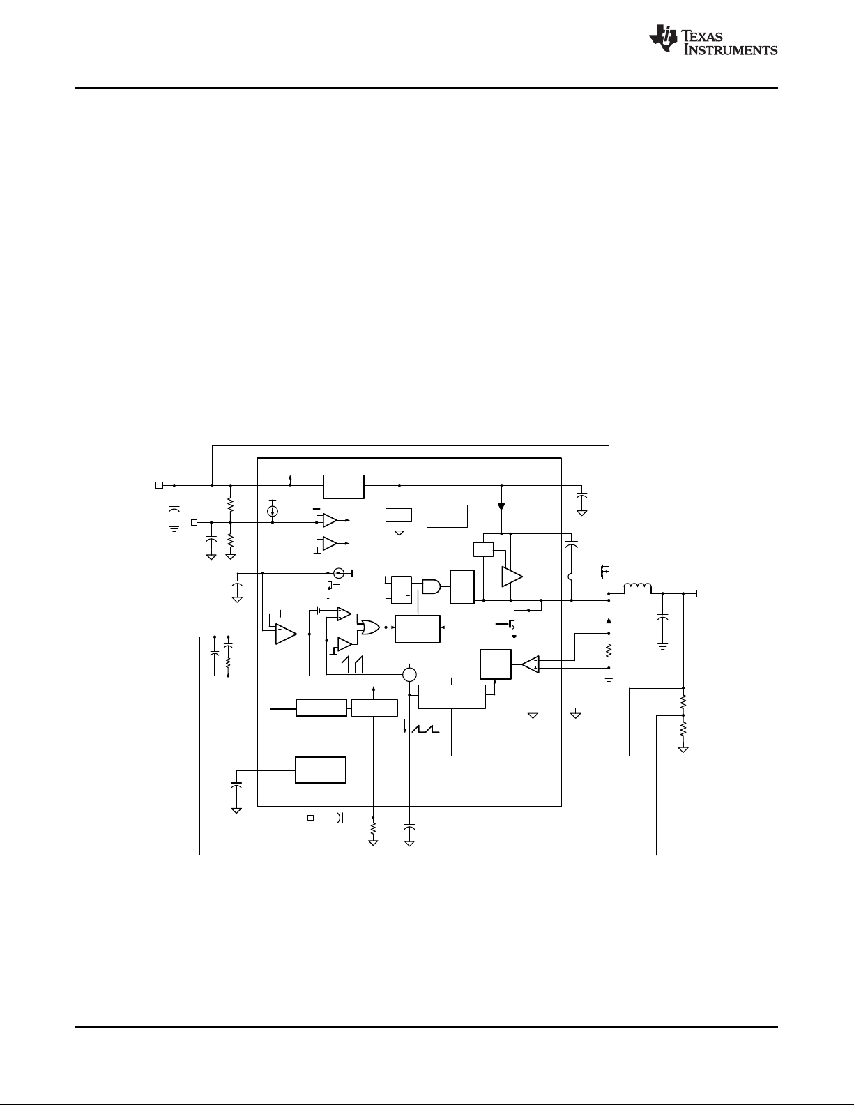
FB
VIN
VCC
SW
RT
Regulator
DRIVER
BOOT
LEVEL
SHIFT
THERMAL
SHUTDOWN
UVLO
ERROR
AMP
DIS
COMP
TRACK
SAMPLE
and
HOLD
CLK
GND
CLK
CSG
CS
CLK
RAMP GENERATOR
+
SHUTDOWN
PWM
I-LIMIT
OUT
RAMP
SS
VIN
STANDBY
5uA
1.2
VIN
EN
Ir
HG
CLK
S
R
Q
Q
CLK
FREQUENCY
DITHERING
STANDBY
SYNC
DITHER
LM5088-1 ONLY
OSCILLATOR
HICCUP
RESTART
LOGIC
Rs
R
FB1
DITHER
RES
R
FB2
Q
L
D
VOUT
C
BOOT
UVLO
MINIMUM
OFF-TIME
LOGIC
7.7V
HICCUP RESTART
LM5088 -2 ONLY
5V
A = -10
C
RES/DITH
C
SYNC
1.2V
R
UV2
R
UV1
C
FT
C
IN
C
SS
C
HF
R
COMP
C
COMP
R
RT
C
RAMP
C
OUT
0.9V
0.4V
5V
11 uA
C
VCC
LM25088
VIN (4.5V-42V)
1.205V
LM25088
,
LM25088-Q1
SNVS609J –DECEMBER 2008–REVISED JANUARY 2015
www.ti.com
8 Detailed Description
8.1 Overview
The LM25088 Wide Input Range Buck Controller features all the functions necessary to implement an efficient
high voltage step-down converter using a minimum number of external components. The control method is
based on peak current mode control utilizing an emulated current ramp. Peak current mode control provides
inherent line voltage feed-forward, cycle-by-cycle current limiting and ease of loop compensation. The use of an
emulated control ramp reduces noise sensitivity of the pulse-width modulation circuit, allowing reliable processing
of very small duty cycles necessary in high input voltage applications. The operating frequency is user
programmable from 50 kHz to 1 MHz. The LM25088-1 provides a ±5% frequency dithering function to reduce the
conducted and radiated EMI, while the LM25088-2 provides a versatile restart timer for overload protection.
Additional features include the low dropout bias regulator, tri-level enable input to control shutdown and standby
modes, soft-start, and voltage tracking and oscillator synchronization capability. The device is available in a
thermally enhanced HTSSOP-16 pin package.
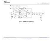
See Figure 13 and Figure 27. The LM25088 is well suited for a wide range of applications where efficient step-
down of high, unregulated input voltage is required. The LM25088’s typical applications include Telecom,
Industrial and Automotive.
8.2 Functional Block Diagram
Figure 13. LM25088 Functional Block Diagram
10 Submit Documentation Feedback Copyright © 2008–2015, Texas Instruments Incorporated
Product Folder Links: LM25088 LM25088-Q1
器件 Datasheet 文档搜索
AiEMA 数据库涵盖高达 72,405,303 个元件的数据手册,每天更新 5,000 多个 PDF 文件
