Datasheet 搜索 > 电压基准芯片 > TI(德州仪器) > LMV431BIMF/NOPB 数据手册 > LMV431BIMF/NOPB 数据手册 5/31 页

¥ 1.976
LMV431BIMF/NOPB 数据手册 - TI(德州仪器)
制造商:
TI(德州仪器)
分类:
电压基准芯片
封装:
SOT-23-3
描述:
TEXAS INSTRUMENTS LMV431BIMF/NOPB 电压基准, 精密, 分流 - 可调, LMV431B系列, 1.24V至30V, SOT-23-3
Pictures:
3D模型
符号图
焊盘图
引脚图
产品图
页面导航:
引脚图在P3Hot
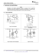
典型应用电路图在P1P16P17
原理图在P15
封装尺寸在P20P21P23P24P25
标记信息在P20P21
封装信息在P19P20P21P22P23P24P25
技术参数、封装参数在P4
应用领域在P1P31
电气规格在P5P6P7P8P9P10P11P12P13P14

导航目录
LMV431BIMF/NOPB数据手册
Page:
of 31 Go
若手册格式错乱,请下载阅览PDF原文件
Z
Z Z
Z
V
R1
r r 1
I R2
'
ª º
§ ·
#
¨ ¸
« »
'
© ¹
¬ ¼
Z
Z
Z
V
r
I
'
'
6
REF
6.0 mV
10
1240 mV
V 39 ppm/ C
125 C
§ ·
¨ ¸
© ¹
v q
q
6 6
Max Min
DEV
REF REF
REF
2 1 2 1
V V
V
10 10
V (at 25 C) V (at 25 C)
ppm
V
C T T T T
§ · § ·
r r
¨ ¸ ¨ ¸
q q
© ¹ © ¹
v
q
REF
Z
V
V
'
'
LMV431
,
LMV431A
,
LMV431B
www.ti.com
SNVS041G –MAY 2004–REVISED SEPTEMBER 2014
7.5 LMV431C Electrical Characteristics
T
A
= 25°C unless otherwise specified
SYMBOL PARAMETER TEST CONDITIONS MIN TYP MAX UNIT
T
A
= 25°C 1.222 1.24 1.258
V
Z
= V
REF
, I
Z
= 10 mA
V
REF
Reference Voltage V
(See Figure 32 )
T
A
= Full Range 1.21 1.27
Deviation of Reference Input Voltage V
Z
= V
REF
, I
Z
= 10 mA,
V
DEV
4 12 mV
Over Temperature
(1)
T
A
= Full Range (See Figure 32)
Ratio of the Change in Reference I
Z
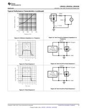
= 10 mA (see Figure 33 )
Voltage to the Change in Cathode V
Z
from V
REF
to 6 V −1.5 −2.7 mV/V
Voltage R
1
= 10 kΩ, R
2
= ∞ and 2.6 kΩ
R
1
= 10 kΩ, R
2
= ∞
I
REF
Reference Input Current 0.15 0.5 μA
I
I
= 10 mA (see Figure 33)
Deviation of Reference Input Current R
1
= 10 kΩ, R
2
= ∞,
∝I
REF
0.05 0.3 μA
over Temperature I
I
= 10 mA, T
A
= Full Range (see Figure 33)
Minimum Cathode Current for
I
Z(MIN)
V
Z
= V
REF
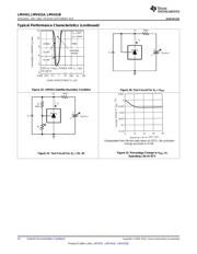
(see Figure 32) 55 80 µA
Regulation
I
Z(OFF)
Off-State Current V
Z
= 6 V, V
REF
= 0 V (see Figure 34 ) 0.001 0.1 μA
V
Z
= V
REF
, I
Z
= 0.1 mA to 15 mA
r
Z
Dynamic Output Impedance
(2)
0.25 0.4 Ω
Frequency = 0 Hz (see Figure 32)
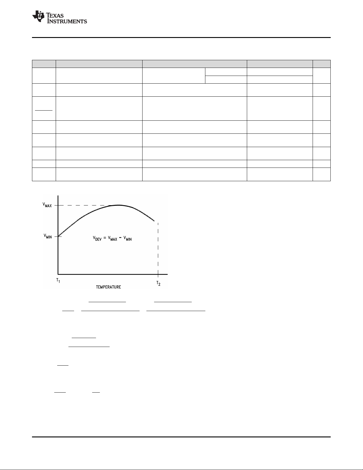
(1) Deviation of reference input voltage, V
DEV
, is defined as the maximum variation of the reference input voltage over the full temperature
range. See the following:
The average temperature coefficient of the reference input voltage, ∝V
REF
, is defined as:
Where: T
2
− T
1
= full temperature change. ∝V
REF
can be positive or negative depending on whether the slope is positive or negative.
Example: V
DEV
= 6 mV, V
REF
= 1240 mV, T
2
− T
1
= 125°C.
(2) The dynamic output impedance, r
Z
, is defined as:
When the device is programmed with two external resistors, R1 and R2, (see Figure 33 ), the dynamic output impedance of the overall
circuit, r
Z
, is defined as:
Copyright © 2004–2014, Texas Instruments Incorporated Submit Documentation Feedback 5
Product Folder Links: LMV431 LMV431A LMV431B
器件 Datasheet 文档搜索
AiEMA 数据库涵盖高达 72,405,303 个元件的数据手册,每天更新 5,000 多个 PDF 文件
