Datasheet 搜索 > DA转换器 > ADI(亚德诺) > AD5360BCPZ-REEL7 数据手册 > AD5360BCPZ-REEL7 开发手册 1/2 页
 器件3D模型
¥ 135.855
AD5360BCPZ-REEL7 开发手册 - ADI(亚德诺)
制造商:
ADI(亚德诺)
分类:
DA转换器
封装:
LFCSP-56
描述:
数模转换器- DAC 16-CH 16-bit Serial bipolar IC
Pictures:
3D模型
符号图
焊盘图
引脚图
产品图
AD5360BCPZ-REEL7数据手册
Page:
of 2 Go
若手册格式错乱,请下载阅览PDF原文件
AN-0986
APPLICATION NOTE
One Technology Way • P. O. Box 9106 • Norwood, MA 02062-9106, U.S.A. • Tel: 781.329.4700 • Fax: 781.461.3113 • www.analog.com
Adjusting the Output Range and Span of the AD5362
by Ken Kavanagh
Rev. 0 | Page 1 of 2
INTRODUCTION
This application note describes how the features of the AD5362
can be used to set up different output ranges on the DAC channels.
While this application note uses the AD5362 as an example, the
methods are also valid for the AD5360, the AD5361, and the
AD5363. The relevant data sheet should be used in conjunction
with this application note. Being able to set up different output
ranges on different channels can be advantageous in PLC and
analog I/O applications because it allows the user to use the full
16-bit digital code range (0 to 65,535) regardless of the output
range of the DAC.
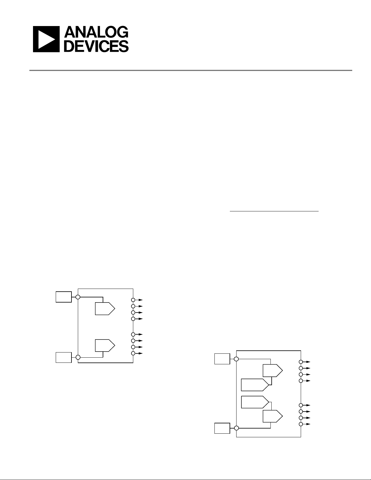
USING THE REFERENCE TO SELECT AN OUTPUT
SPAN
In its default operating condition, the AD5362 produces a bipolar
output span that is four times the reference value. For example,
a 5 V reference gives a span of ±10 V, and a 3 V reference gives a
span of ±6 V. The AD5362 has two independent reference input
pins, VREF0 and VREF1. VREF0 is the reference source for
DAC 0 to DAC 3, and VREF1 is the reference source for DAC 4
to DAC 7. Figure 1 shows how the separate reference values can
be used to implement different DAC output ranges.
VREF0
VOUT0
±10V
±10V
±10V
±10V
±5V
±5V
±5V
±5V
VOUT1
VOUT2
VOUT4
VOUT5
VOUT6
VOUT7
VOUT3
VREF1
5.0V
2.5V
DAC 0
TO
DAC 3
DAC 4
TO
DAC 7
07878-001
Figure 1. Using Sep
arate References
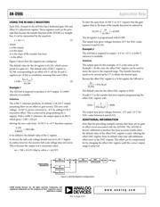
CHANGING THE OUTPUT RANGE
By default, the DAC outputs swing positive and negative around
0 V. The center point of the span can be altered to give output
ranges that do not necessarily center at 0 V. This is achieved by
programming the offset DAC r
egisters. There are two offset
DAC re
gisters in the AD5362. OFS0 controls the offset of DAC 0
to DAC 3 and OFS1 controls the offset of DAC 4 to DAC 7. The
offset DACs in the AD5362 are 14-bit DACs and have a span of
four times the reference value. In theory, this allows the user to
move the output span up or down by up to 10 V. However, the
outputs can only be adjusted within the limits of the supplies
and headroom requirements. For example, using a 2.5 V refer-
ence, the nominal ±5 V output can be offset to produce either
a −10 V to 0 V or 0 V to +10 V output. However, with a 5 V
reference, producing a nominal ±10 V output, the offset DAC
registers cannot be used to generate a 0 V to +20 V output because
this violates the power supply and headroom limitations.
The output voltage of any DAC channel is governed by the
following formula:
( )
SIGGND
REF
OUT
V
CODEOFFSETCODEDAC
VV
+
×−
××=
16
2
_4_
4
where:
DAC_CODE is the data written to the X1A or X1B register of a
DAC. It should be within the range of 0 to 65,535.
OFFSET_CODE is the value loaded to the relevant offset DAC
register. It should be in the range of 0 to 16,383. Note that the
OFFSET_CODE is multiplied by 4 in the equation because the
offset DAC has 14 bits of resolution and the AD5362 DACs
have 16 bits of resolution.
V
REF
is the reference voltage and is in the range of 2.0 V to 5.0 V.
V
SIGGND
is the voltage on the relevant SIGGND pin. This is
normally 0 V.
The default value of the offset DAC register is 8192. This gives a
voltage output that is bipolar and centered around 0 V. It can be
seen from the preceding equation that values above 8192 move
the center of the span below 0 V and values below 8192 move
the center of the span above 0 V. Figure 2 shows how the offset
DACs can be used to set up different ranges on different DACs.
VREF0
VOUT0
–8V TO +12V
–8V TO +12V
–8V TO +12V
–8V TO +12V
0V TO +10V
0V TO +10V
0V TO +10V
0V TO +10V
VOUT1
VOUT2
VOUT4
VOUT5
VOUT6
VOUT7
VOUT3
VREF1
5.0V
2.5V
DAC 0
TO
DAC 3
DAC 4
TO
DAC 7
07878-002
OFS0 = 6553
OFS1 = 0
Figure 2. Generating Different Output Ranges
器件 Datasheet 文档搜索
AiEMA 数据库涵盖高达 72,405,303 个元件的数据手册,每天更新 5,000 多个 PDF 文件
