Datasheet 搜索 > 放大器、缓冲器 > ADI(亚德诺) > AD844SQ 数据手册 > AD844SQ 开发手册 5/8 页
 器件3D模型
¥ 198.726
AD844SQ 开发手册 - ADI(亚德诺)
制造商:
ADI(亚德诺)
分类:
放大器、缓冲器
封装:
CDIP-8
描述:
60兆赫, 2000 V / us的单片运算放大器 60 MHz, 2000 V/us Monolithic Op Amp
Pictures:
3D模型
符号图
焊盘图
引脚图
产品图
页面导航:
应用领域在P1P6
型号编号列表在P5
导航目录
AD844SQ数据手册
Page:
of 8 Go
若手册格式错乱,请下载阅览PDF原文件

–5–
AN-581
REV. 0
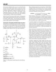
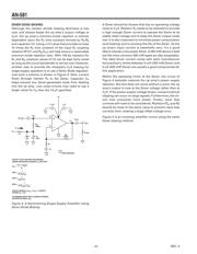
BW1 =
1
2
π
R1 C1
BW2 =
1
2
π
R
IN
C2
WHERE X
C1
<<R1
BW3 =
1
2
π
R
LOAD
C
OUT
TO MINIMIZE INPUT BIAS CURRENT ERRORS,
R2 SHOULD EQUAL R
IN
.
R
Z
=
+V
S
– V
ZENER
I
Z
SELECT R
Z
TO PROVIDE THE DESIRED
ZENER OPERATING CURRENT, I
Z
.
SEE TEXT.
FOR AC SIGNALS, V
OUT
= V
IN
(R2/R1)
0.1F
1F
*
*
V
S
R1
*STAR GROUND
C
OUT
V
OUT
R
LOAD
R
IN
100k
R2
100k
C1
V
IN
V
Z
V
Z
V
S
I
Z
R
Z
ZENER
V
Z
*
*
C2
10 F
+
Figure 5. An Inverting Single Supply Amplifier Using
Zener Diode Biasing
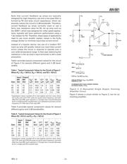
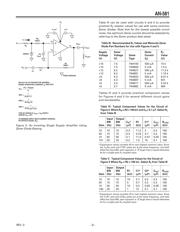
Table III can be used with circuits 4 and 5 to provide
practical R
Z
resistor values for use with some common
Zener diodes. Note that for the lowest possible circuit
noise, the optimum Zener current should be selected by
referring to the Zener product data sheet.
Table III. Recommended R
Z
Values and Motorola Zener
Diode Part Numbers for Use with Figures 4 and 5
Supply Zener Zener R
Z
Voltage Voltage Zener Current Value
(V) (V) Type (I
Z
)()
+15 7.5 1N4100 500 µA 15 k
+15 7.5 1N4693 5 mA 1.5 k
+12 6.2 1N4627 500 µA 11.5 k
+12 6.2 1N4691 5 mA 1.15 k
+9 4.3 1N4623 500 µA 9.31 k
+9 4.3 1N4687 5 mA 931
+5 2.4 1N4617 500 µA 5.23 k
+5 2.7 1N4682 5 mA 464
Tables IV and V provide practical component values
for Figures 4 and 5 for several different circuit gains
and bandwidths.
Table IV. Typical Component Values for the Circuit of
Figure 4 Where R
IN
= R2 = 100 k and C
N
= 0.1 F. Select R
Z
from Table III
Input Output
BW BW C
IN
*R1 C1* C
OUT
R
LOAD
Gain (Hz) (Hz) (F) (k)(F) (F) (k)
10 10 10 0.3 11.0 2 0.2 100
20 10 10 0.3 5.23 4.7 0.2 100
10 50 50 0.1 11.0 0.47 0.05 100
101 20 20 0.2 1.0 15 0.1 100
*Capacitance values rounded off to next highest common value. Since
the C
IN
/R
IN
pole and C1/R1 poles are at the same frequency, and both
affect the input BW, each capacitor is √2 larger than it would otherwise
be for a single pole R
C
-coupled input.
Table V. Typical Component Values for the Circuit of
Figure 5 Where R
IN
= R2 = 100 k. Select R
Z
from Table III
Input Output
BW BW R1 C1* C2* C
OUT
R
LOAD
Gain (Hz) (Hz) (k)(F) (F) (F) (k)
10 10 10 10 2.7 0.2 0.2 100
20 10 10 5 4.7 0.2 0.2 100
10 50 50 10 0.5 0.05 0.05 100
100 20 20 1 12 0.1 0.1 100
*Capacitance values rounded off to next highest common value. Since
the C1/R1 pole and C2/R
IN
poles are at the same frequency, and both
affect the input BW, each capacitor is √2 larger than it would otherwise
be for a single pole R
C
-coupled input.
器件 Datasheet 文档搜索
AiEMA 数据库涵盖高达 72,405,303 个元件的数据手册,每天更新 5,000 多个 PDF 文件
