Datasheet 搜索 > 放大器、缓冲器 > ADI(亚德诺) > AD847JRZ-REEL7 数据手册 > AD847JRZ-REEL7 开发手册 1/8 页

 器件3D模型
¥ 20.87
AD847JRZ-REEL7 开发手册 - ADI(亚德诺)
制造商:
ADI(亚德诺)
分类:
放大器、缓冲器
封装:
SOIC-8
描述:
高速,低功耗单片运算放大器 High Speed, Low Power Monolithic Op Amp
Pictures:
3D模型
符号图
焊盘图
引脚图
产品图
页面导航:
应用领域在P1P6
型号编号列表在P5
导航目录
AD847JRZ-REEL7数据手册
Page:
of 8 Go
若手册格式错乱,请下载阅览PDF原文件
REV. 0
a
AN-581
APPLICATION NOTE
One Technology Way • P.O. Box 9106 • Norwood, MA 02062-9106 • Tel: 781/329-4700 • Fax: 781/326-8703 • www.analog.com
Biasing and Decoupling Op Amps
in Single Supply Applications
by Charles Kitchin
© Analog Devices, Inc., 2002
SINGLE OR DUAL SUPPLY?
Battery-powered op amp applications such as those
found in automotive and marine equipment have only a
single available power source. Other applications, such
as computers, may operate from the ac power lines but
still have only a single polarity power source, such as
5 V or 12 V dc. Therefore, it is often a practical necessity
to power op amp circuits from a single polarity supply.
But single supply operation does have its drawbacks: it
requires additional passive components in each stage
and, if not properly executed, can lead to serious insta-
bility problems.
COMMON PROBLEMS WITH RESISTOR BIASING
Single supply applications have inherent problems that
are not usually found in dual supply op amp circuits. The
fundamental problem is that an op amp is a dual supply
device and so some type of biasing, using external com-
ponents, must be used to center the op amp’s output
voltage at midsupply. This allows the maximum input
and output voltage swing for a given supply voltage.
In some low gain applications, where input signals are
very small, the op amp’s output can be lifted above
ground by only 2 V or 3 V. But in most cases, all clipping
needs to be avoided and so the output needs to be cen-
tered around midsupply.
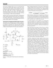
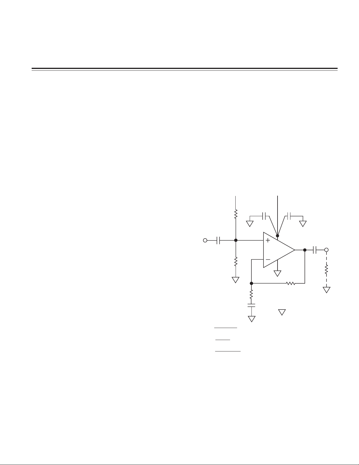
The circuit of Figure 1 shows a simple single supply
biasing method. This noninverting, ac-coupled, ampli-
fier circuit uses a resistor divider with two biasing
resistors, R
A
and R
B
, to set the voltage on the noninvert-
ing equal to V
S
/2. As shown, the input signal, V
IN
, is
capacitively coupled to the noninverting input terminal.
This simple circuit has some serious limitations. One is
that the op amp’s power supply rejection is almost entirely
gone, as any change in supply voltage will directly
change the V
S
/2 biasing voltage set by the resistor divider.
Power Supply Rejection (PSR) is a very important (and
frequently overlooked) op amp characteristic.
Since a one volt change on the supply line causes a
one-half volt change at the output of the divider, the
circuit’s PSR is only 6 dB. So, the normally high power
supply rejection provided by any modern op amp,
which greatly reduces any ac signals (and power sup-
ply hum) from feeding into the op amp via its supply
line, is now gone.
0.1F
1F
V
S
R2
R1
C1
*STAR GROUND
C
OUT
V
OUT
R
LOAD
V
S
/2
V
S
/2
R
A
100k
R
B
100k
*
*
V
S
C
IN
V
IN
π ( )
BW1
=
1
2
π 1/2R
A
C
IN
BW2 =
1
2
π R1 C1
BW3 =
1
2
π R
LOAD
C
OUT
FOR R
A
= R
B
FOR AC SIGNALS, V
OUT
= V
IN
(1 + (R2/R1))
WHERE X
C1
<<
R1
*
*
Figure 1. A Potentially Unstable Single Supply Op
Amp Circuit
器件 Datasheet 文档搜索
AiEMA 数据库涵盖高达 72,405,303 个元件的数据手册,每天更新 5,000 多个 PDF 文件
