Datasheet 搜索 > AD转换器 > TI(德州仪器) > ADS1114IDGST 数据手册 > ADS1114IDGST 开发手册 1/21 页

 器件3D模型
¥ 35.073
ADS1114IDGST 开发手册 - TI(德州仪器)
制造商:
TI(德州仪器)
分类:
AD转换器
封装:
VSSOP-10
描述:
TEXAS INSTRUMENTS ADS1114IDGST 模数转换器, 16 bit, 860 SPS, 单, 2 V, 5.5 V, VSSOP
Pictures:
3D模型
符号图
焊盘图
引脚图
产品图
页面导航:
封装尺寸在P5
焊接温度在P4P13P14P15
应用领域在P21
导航目录
ADS1114IDGST数据手册
Page:
of 21 Go
若手册格式错乱,请下载阅览PDF原文件
Application Report
SLUA271A – June 2002 – Revised September 2007
QFN/SON PCB Attachment
Steve Kummerl, Bernhard Lange, Dominic Nguyen .................................................................................
ABSTRACT
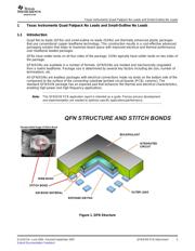
Quad flatpack no leads (QFNs) and small-outline no leads (SONs) are leadless
packages with electrical connections made via lands on the bottom side of the
component to the surface of the connecting substrate (PCB, ceramic). This application
report presents users with introductory information about attaching QFN/SON devices
to printed circuit boards (PCBs).
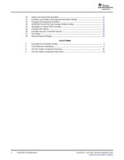
Contents
1 Texas Instruments Quad Flatpack No Leads and Small-Outline No Leads ................ 3
2 Manufacturing Considerations .................................................................... 4
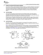
3 Printed Circuit Board (PCB) Design Guidelines ................................................ 5
4 Solder Paste Screen Printing Process ......................................................... 10
5 Package to Board Assembly Process .......................................................... 13
6 Rework Guidelines (Hot Gas Convection and Manual) ...................................... 16
List of Figures
1 QFN Structure ....................................................................................... 3
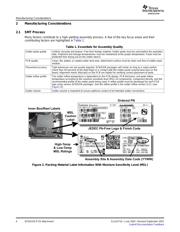
2 Packing Material Label Information With Moisture Sensitivity Level (MSL) ................. 4
3 QFN/SON Outline Dimensions .................................................................... 5
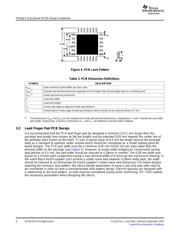
4 PCB Land Pattern .................................................................................. 6
5 Substrate/PCB Lead Finger Geometry .......................................................... 7
6 X-Ray Images for Reference ...................................................................... 8
7 Substrate/PCB Solder Mask and Keep-Out Area Example ................................... 8
8 Avoid Excessive Bending .......................................................................... 9
9 Solder Stencil Profile ............................................................................. 10
SLUA271A – June 2002 – Revised September 2007 QFN/SON PCB Attachment 1
Submit Documentation Feedback
器件 Datasheet 文档搜索
AiEMA 数据库涵盖高达 72,405,303 个元件的数据手册,每天更新 5,000 多个 PDF 文件
