Datasheet 搜索 > 温度传感器 > Maxim Integrated(美信) > DS1631Z 数据手册 > DS1631Z 开发手册 1/6 页

 器件3D模型
¥ 1
DS1631Z 开发手册 - Maxim Integrated(美信)
制造商:
Maxim Integrated(美信)
分类:
温度传感器
封装:
SOIC-8
描述:
高精度数字温度计和温度监控器 High-Precision Digital Thermometer and Thermostat
Pictures:
3D模型
符号图
焊盘图
引脚图
产品图
DS1631Z数据手册
Page:
of 6 Go
若手册格式错乱,请下载阅览PDF原文件

Maxim > Design Support > Technical Documents > Application Notes > Temperature Sensors and Thermal Management > APP 5727
Keywords: temperature sensor, I2C slave addressing, multidrop
APPLICATION NOTE 5727
Understanding Multidrop Address Assignments for
Thermal Sensors
Mar 28, 2014
Abstract:
In
many thermal applications, it may be desired to utilize multiple temperature sensors, placed in
different physical locations, to monitor the operating temperatures in predefined 'zones' within the system. To
accommodate this desire, many thermal products have the added flexibility of user-defined slave addressing.
A similar version was published in the March 2014 issue of Electronics Maker magazine.
Traditionally, most ICs incorporating the Philips
®
I
2
C I/O protocol have a fixed (factory-defined) slave address
for use during communications. In many thermal applications, however, it may be desirable to utilize multiple
temperature sensors, placed in different physical locations, to monitor the operating temperatures in predefined
"zones" within the system. To accommodate this while minimizing CPU resources allocated for
communications functions, many thermal products have the added flexibility of user-defined slave addressing.
This user-defined function uses an additional input pin (or pins) that allows mapping of a specific sensor to a
schematically defined slave address.
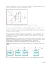
Categorizing the thermal products by its I/O multidrop capability results in three fundamental variations of the
options for user-defined slave addressing:
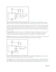
Input-Level Defined. The condition of the address input pin can be controlled by a simple hardware definition
(i.e., resistor placement) or by a dynamic CPU resource. Standard digital logic input levels (V
IH
/V
IL
) utilized on
SCL and SDA can also be applied to the address input pin(s).
Figure 1 depicts a typical I
2
C resistor pullup scheme where the I
2
C master's resource is defined as open
drain, and the default ADD pin state is Logic 1. The desired decode (ADD input bias) must be presented prior
to the associated START signal whenever this slave is to be accessed; it should remain stable until after the
associated STOP has been issued.
Page 1 of 6
器件 Datasheet 文档搜索
AiEMA 数据库涵盖高达 72,405,303 个元件的数据手册,每天更新 5,000 多个 PDF 文件
