Datasheet 搜索 > 计数器 > ON Semiconductor(安森美) > MC14060BDR2G 数据手册 > MC14060BDR2G 开发手册 1/9 页
 器件3D模型
¥ 1.677
MC14060BDR2G 开发手册 - ON Semiconductor(安森美)
制造商:
ON Semiconductor(安森美)
分类:
计数器
封装:
SOIC-16
描述:
ON SEMICONDUCTOR MC14060BDR2G COUNTER, BINARY RIPPLE, 14BIT, SOIC-16 新
Pictures:
3D模型
符号图
焊盘图
引脚图
产品图
页面导航:
导航目录
MC14060BDR2G数据手册
Page:
of 9 Go
若手册格式错乱,请下载阅览PDF原文件
© Semiconductor Components Industries, LLC, 2011
June, 2011 − Rev. 8
1 Publication Order Number:
MC14060B/D
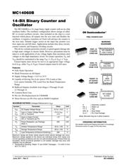
MC14060B
14-Bit Binary Counter and
Oscillator
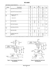
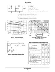
The MC14060B is a 14−stage binary ripple counter with an on−chip
oscillator buffer. The oscillator configuration allows design of either
RC or crystal oscillator circuits. Also included on the chip is a reset
function which places all outputs into the zero state and disables the
oscillator. A negative transition on Clock will advance the counter to
the next state. Schmitt trigger action on the input line permits very
slow input rise and fall times. Applications include time delay circuits,
counter controls, and frequency dividing circuits.
This device contains protection circuitry to guard against damage due
to high static voltages or electric fields. However, precautions must be
taken to avoid applications of any voltage higher than maximum rated
voltages to this high−impedance circuit. For proper operation, V
in
and
V
out
should be constrained to the range V
SS
v (V
in
or V
out
) v V
DD
.
Unused inputs must always be tied to an appropriate logic voltage
level (e.g., either V
SS
or V
DD
). Unused outputs must be left open.
Features
• Fully Static Operation
• Diode Protection on All Inputs
• Supply Voltage Range = 3.0 V to 18 V
• Capable of Driving Two Low−power TTL Loads or One
Low−power Schottky TTL Load Over the Rated Temperature
Range
• Buffered Outputs Available from Stages 4 Through 10 and
12 Through 14
• Common Reset Line
• Pin−for−Pin Replacement for CD4060B
• These Devices are Pb−Free and are RoHS Compliant
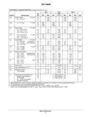
MAXIMUM RATINGS (Voltages Referenced to V
SS
)
Symbol
Parameter Value Unit
V
DD
DC Supply Voltage Range −0.5 to +18.0 V
V
in
,
V
out
Input or Output Voltage Range
(DC or Transient)
−0.5 to V
DD
+0.5
V
I
in
,
I
out
Input or Output Current
(DC or Transient) per Pin
±10 mA
P
D
Power Dissipation, per Package
(Note 1)
500 mW
T
A
Ambient Temperature Range −55 to +125 °C
T
stg
Storage Temperature Range −65 to +150 °C
T
L
Lead Temperature (8 Second Soldering) 260 °C
Maximum ratings are those values beyond which device damage can occur.
Maximum ratings applied to the device are individual stress limit values (not
normal operating conditions) and are not valid simultaneously. If these limits are
exceeded, device functional operation is not implied, damage may occur and
reliability may be affected.
1. Temperature Derating: Plastic “P and D/DW” Packages: –7.0 mW/°C from
65°C To 125°C.
http://onsemi.com
See detailed ordering and shipping information in the package
dimensions section on page 2 of this data sheet.
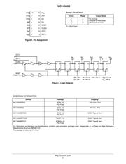
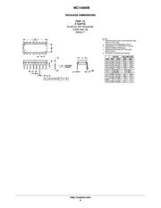
ORDERING INFORMATION
MARKING
DIAGRAMS
PDIP−16
P SUFFIX
CASE 648
MC14060BCP
AWLYYWWG
SOIC−16
D SUFFIX
CASE 751B
TSSOP−16
DT SUFFIX
CASE 948F
14060BG
AWLYWW
SOEIAJ−16
F SUFFIX
CASE 966
MC14060B
ALYWG
16
1
1
16
1
16
14
060B
ALYW G
G
1
16
A = Assembly Location
WL, L = Wafer Lot
YY, Y = Year
WW, W = Work Week
G or G = Pb−Free Package
(Note: Microdot may be in either location)
器件 Datasheet 文档搜索
AiEMA 数据库涵盖高达 72,405,303 个元件的数据手册,每天更新 5,000 多个 PDF 文件
