Datasheet 搜索 > RF模块、IC及配件 > ON Semiconductor(安森美) > MC1496DR2G 数据手册 > MC1496DR2G 开发手册 1/12 页
 器件3D模型
¥ 1.882
MC1496DR2G 开发手册 - ON Semiconductor(安森美)
制造商:
ON Semiconductor(安森美)
分类:
RF模块、IC及配件
封装:
SOIC-14
描述:
ON SEMICONDUCTOR MC1496DR2G 芯片, 平衡调制/解调器, 14SOIC
Pictures:
3D模型
符号图
焊盘图
引脚图
产品图
页面导航:
原理图在P1
型号编码规则在P12
功能描述在P1
应用领域在P1P10


导航目录
MC1496DR2G数据手册
Page:
of 12 Go
若手册格式错乱,请下载阅览PDF原文件

Semiconductor Components Industries, LLC, 2002
January, 2002 – Rev. 3
1 Publication Order Number:
AN531/D
AN531/D
MC1496 Balanced
Modulator
Prepared by: Roy Hejhall
Applications Engineering
INTRODUCTION
The ON Semiconductor MC1496 monolithic balanced
modulator makes an excellent building block for high
frequency communications equipment.
The device functions as a broadband, double–sideband
suppressed carrier balanced modulator without a
requirement for transformers or tuned circuits. In addition to
its basic application as a balanced modulator/demodulator,
the device offers excellent performance as an SSB product
detector, AM modulator/detector, FM detector, mixer,
frequency doubler, phase detector, and more.
The article consists of a general description of the
MC1496, its gain equations, biasing information, and
circuits illustrating typical applications. It is followed by an
appendix containing a detailed mathematical ac and dc
analysis of the device.
Many readers may find that one of the circuits described
in the article will fill the needs of their application. However,
it is impossible to show typical circuits for every possible
requirement, and the detailed analysis given in the appendix
will assist the designer in developing an optimum circuit
for any application within the basic capabilities of the
MC1496.
MC1496 General Description
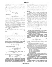
Figure 1 shows a schematic diagram of the MC1496. For
purposes of the analysis, the following conventional
assumptions have been made for simplification: (1) Devices
of similar geometry within a monolithic chip are assumed
identical and matched where necessary, and (2) transistor
base currents are ignored with respect to the magnitude of
collector currents; therefore, collector and emitter currents
are assumed equal.
Referring to Figures 1 and 2, the MC1496 consists of
differential amplifier Q5–Q6 driving a dual differential
amplifier composed of transistors Q1, Q2, Q3 and Q4.
Transistors Q7 and Q8 and associated bias circuitry form
constant current sources for the lower differential amplifier
Q5–Q6.
The analysis of operation of the MC1496 is based on the
ability of the device to deliver an output which is proportional
to the product of the input voltages V
X
and V
Y
. This holds true
when the magnitudes of V
X
and V
Y
are maintained within the
limits of linear operation of the three differential amplifiers in
the device. Expressed mathematically, the output voltage
(actually output current, which is converted to an output
voltage by an external load resistance), V
O
is given by
V
O
KV
X
V
Y
(1)
10(–)
8(+)
4(–)
1(+)
(–)12
(+)6
Q1 Q2 Q3
Q5 Q6
Q7
Q8
Q4
2
3
500500500
Carrier
Input
Signal
Input
V
C
V
S
Bias 5
V
–
14
V
O
, Output
Gain Adjust
Figure 1. MC1496 Schematic
http://onsemi.com
APPLICATION NOTE
器件 Datasheet 文档搜索
AiEMA 数据库涵盖高达 72,405,303 个元件的数据手册,每天更新 5,000 多个 PDF 文件
