Datasheet 搜索 > AD转换器 > Microchip(微芯) > MCP3208-BI/SL 数据手册 > MCP3208-BI/SL 开发手册 1/11 页
 器件3D模型
¥ 37.966
MCP3208-BI/SL 开发手册 - Microchip(微芯)
制造商:
Microchip(微芯)
分类:
AD转换器
封装:
SOIC-16
描述:
MICROCHIP MCP3208-BI/SL 模数转换器, 八路, AEC-Q100, 12 bit, 100 kSPS, 单, 2.7 V, 5.5 V, SOIC
Pictures:
3D模型
符号图
焊盘图
引脚图
产品图
页面导航:
技术参数、封装参数在P1P3P5P7
应用领域在P9

导航目录
MCP3208-BI/SL数据手册
Page:
of 11 Go
若手册格式错乱,请下载阅览PDF原文件
2000 Microchip Technology Inc. Preliminary DS00693A-page 1
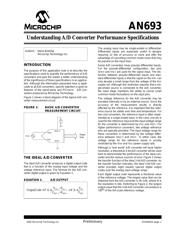
AN693
INTRODUCTION
The purpose of this application note is to describe the
specifications used to quantify the performance of A/D
converters and give the reader a better understanding
of the significance of those specifications in an applica-
tion. Although the information presented here is appli-
cable to all A/D converters, specific attention is given to
features of the stand-alone and PICmicro
A/D con-
verters produced by Microchip Technology.
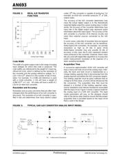
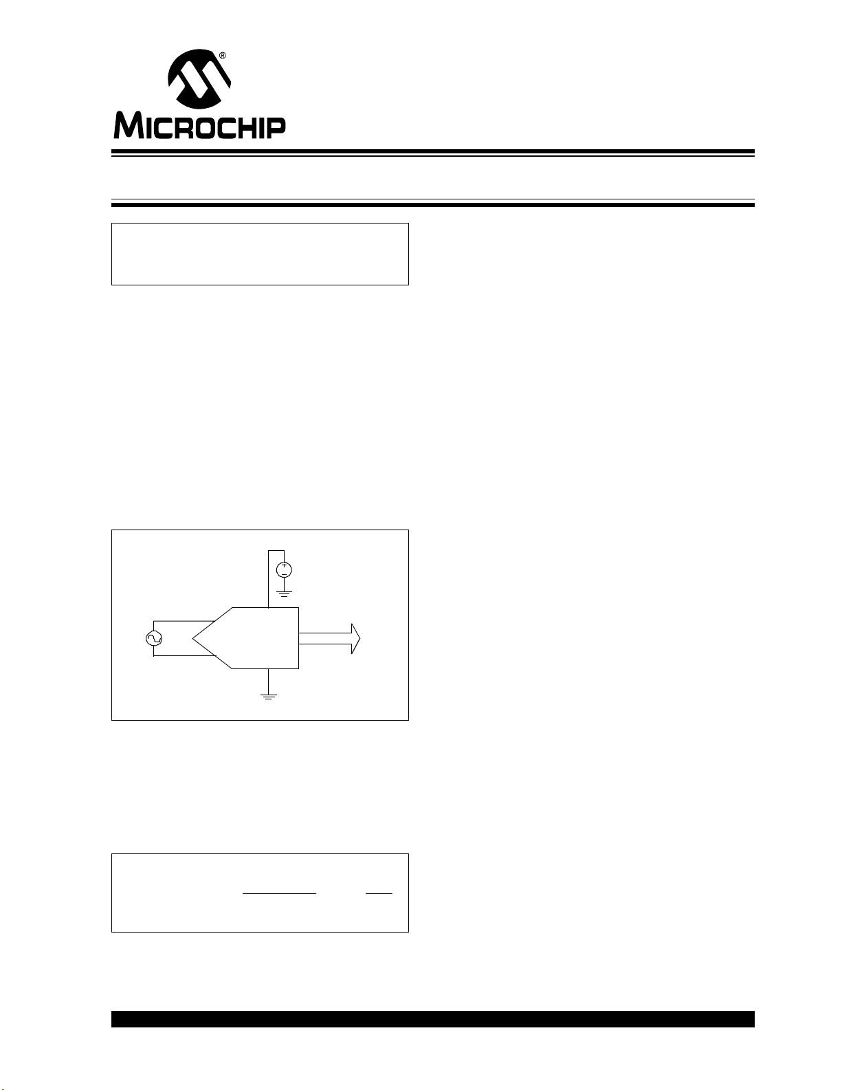
Figure 1 shows a block diagram of the typical A/D con-
verter measurement circuit.
FIGURE 1: BASIC A/D CONVERTER
MEASUREMENT CIRCUIT
THE IDEAL A/D CONVERTER
The ideal A/D converter produces a digital output code
that is a function of the analog input voltage and the
voltage reference input. The formula for the A/D con-
verter digital output is given by Equation 1.
EQUATION 1: A/D OUTPUT
The analog input may be single-ended or differential.
Differential inputs are especially useful in designs
requiring 12 bits of accuracy or more and offer the
advantage of cancelling common mode noise that may
be present on the input lines.
Some A/D converters have pseudo-differential inputs.
For the pseudo-differential configuration, two pins
(V
IN+ and VIN-) are used for the signal input. The dis-
tinction between pseudo-differential inputs and stan-
dard differential inputs is that the signal on the VIN- can
only deviate a small range from the voltage of the V
SS
supply rail. Although this restriction requires that a sin-
gle-ended source is connected to the A/D converter,
the input stage maintains the ability to cancel small
common-mode fluctuations on the input pins.
The voltage reference for the A/D converter may be
provided internally or by an external source. Since the
accuracy of the measurement results is directly
affected by the reference, it is important that the refer-
ence source be stable over time and temperature. For
low cost converters, the reference input is often imple-
mented as a single-ended input. In this case, one pin is
used for the reference input and the input voltage range
for the converter is determined by V
SS and VREF. For
higher performance converters, two voltage reference
pins are typically provided. The input voltage range for
these converters is determined by the voltage differ-
ence between V
REF+ and VREF-. In either case, the
voltage range for the reference inputs is usually
restricted by the VDD and VSS power supply rails.
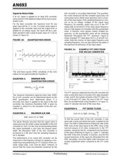
Although a “real world” A/D converter will have higher
resolution, a theoretical 3-bit A/D converter will be used
here to demonstrate the performance of the ideal con-
verter and the various sources of error. Figure 2 shows
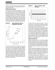
the transfer function of the ideal 3-bit A/D converter. As
the transfer function indicates, the ideal 3-bit A/D con-
verter provides eight equally spaced digital output
codes over the analog input voltage range.
Each digital output code represents a fractional value
of the reference voltage. The largest value that can be
obtained from the A/D converter is (N-1)/N, where N is
the resolution in bits. Referring to Figure 2, the largest
output value that the 3-bit A/D converter can produce is
7/8
ths
of the full-scale reference voltage.
Authors: Steve Bowling
Microchip Technology Inc.
VSIG
VREF+
V
REF-
VIN+
Digital
Data
VIN-
REF
IN
REFREF
ININ
V
V
SF
VV
VV
SFOutputCode ×=
−
−
×=
−+
−+
....
Understanding A/D Converter Performance Specifications
器件 Datasheet 文档搜索
AiEMA 数据库涵盖高达 72,405,303 个元件的数据手册,每天更新 5,000 多个 PDF 文件
