Datasheet 搜索 > Zarlink(英商卓联) > MT9074AL 数据手册 > MT9074AL 开发手册 4/124 页


¥ 0
MT9074AL 开发手册 - Zarlink(英商卓联)
制造商:
Zarlink(英商卓联)
Pictures:
3D模型
符号图
焊盘图
引脚图
产品图
MT9074AL数据手册
Page:
of 124 Go
若手册格式错乱,请下载阅览PDF原文件
Data Sheet MT9074
4
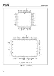
Pin Description
Pin #
Name Description
68 Pin
PLCC
100 Pin
MQFP
1 66 OSC1 Oscillator Input. This pin is either connected via a 20.000 MHz crystal to OSC2
where a crystal is used, or is directly driven when a 20.000 MHz. oscillator is
employed.
2 67 OSC2 Oscillator Output. Connect a 20.0 MHz crystal between OSC1 and OSC2. Not
suitable for driving other devices.
368 V
SS
Negative Power Supply (Input). Digital ground.
469 V
DD
Positive Power Supply (Input). Digital supply (+5V ± 5%).
5 70 CSTo Control ST-BUS Output. CSTo carries serial streams for CAS and CCS
respectively a 2.048 Mbit/s ST-BUS status stream which contains the 30 receive
signaling nibbles (ABCDZZZZ or ZZZZABCD). The most significant nibbles of
each ST-BUS time slot are valid and the least significant nibbles of each ST-BUS
time slot are tristated when control bit MSN (page 01H, address 1AH, bit 1) is set
to 1. If MSN=0, the position of the valid and tristated nibbles are reversed.
6 71 CSTi Control ST-BUS Input. CSTi carries serial streams for CAS and CCS respectively
a 2.048 Mbit/s ST-BUS control stream which contains the 30 transmit signaling
nibbles (ABCDXXXX or XXXXABCD) when RPSIG=0. When RPSIG=1 this pin
has no function. The most significant nibbles of each ST-BUS time slot are valid
and the least significant nibbles of each ST-BUS time slot are ignored when control
bit MSN (page 01H, address 1AH, bit 1) is set to 1. If MSN=0, the position of the
valid and ignored nibbles is reversed.
7 72 DSTo Data ST-BUS Output. A 2.048 Mbit/s serial stream which contains the 24/30
PCM(T1/E1) or data channels received on the PCM24/30 (T1/E1) line.
8 73 DSTi Data ST-BUS Input. A 2.048 Mbit/s serial stream which contains the 24/30 (T1/
E1)PCM or data channels to be transmitted on the PCM24/30 (T1/E1)line.
974DS
/RD Data/Read Strobe (Input).
In Motorola mode (DS
), this input is the active low data strobe of the
microprocessor interface.
In Intel mode (RD
), this input is the active low read strobe of the microprocessor
interface.
10 83 CS
Chip Select (Input). This active low input enables the non-multiplexed parallel
microprocessor interface of the MT9074. When CS
is set to high, the
microprocessor interface is idle and all bus I/O pins will be in a high impedance
state.
11 84 RESET
RESET (Input). This active low input puts the MT9074 in a reset condition. RESET
should be set to high for normal operation. The MT9074 should be reset after
power-up. The RESET
pin must be held low for a minimum of 1µsec. to reset the
device properly.
12 85 IRQ
Interrupt Request (Output). A low on this output pin indicates that an interrupt
request is presented. IRQ
is an open drain output that should be connected to V
DD
through a pull-up resistor. An active low CS signal is not required for this pin to
function.
13 -
16
86-89 D0 - D3 Data 0 to Data 3 (Three-state I/O). These signals combined with D4-D7 form the
bidirectional data bus of the microprocessor interface (D0 is the least significant
bit).
器件 Datasheet 文档搜索
AiEMA 数据库涵盖高达 72,405,303 个元件的数据手册,每天更新 5,000 多个 PDF 文件
