Datasheet 搜索 > 逻辑芯片 > ON Semiconductor(安森美) > NB7L86MMNR2 数据手册 > NB7L86MMNR2 开发手册 1/12 页

¥ 0
NB7L86MMNR2 开发手册 - ON Semiconductor(安森美)
制造商:
ON Semiconductor(安森美)
分类:
逻辑芯片
封装:
VFQFN-16
描述:
2.5V / 3.3V 12 Gb / s的差分时钟/数据Smartgate的与CML输出和内部终端 2.5V/3.3V 12 Gb/s Differential Clock/Data SmartGate with CML Output and Internal Termination
Pictures:
3D模型
符号图
焊盘图
引脚图
产品图
页面导航:
导航目录
NB7L86MMNR2数据手册
Page:
of 12 Go
若手册格式错乱,请下载阅览PDF原文件
© Semiconductor Components Industries, LLC, 2012
March, 2012 − Rev. 7
1 Publication Order Number:
NB7L86M/D
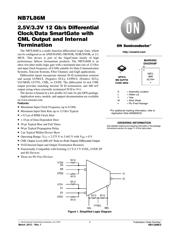
NB7L86M
2.5V/3.3V 12 Gb/s Differential
Clock/Data SmartGate with
CML Output and Internal
Termination
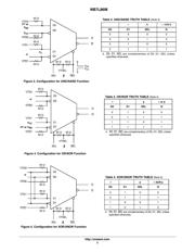
The NB7L86M is a multi−function differential Logic Gate, which
can be configured as an AND/NAND, OR/NOR, XOR/XNOR, or 2:1
MUX. This device is part of the GigaComm family of high
performance Silicon Germanium products. The NB7L86M is an
ultra−low jitter multi−logic gate with a maximum data rate of 12 Gb/s
and input clock frequency of 8 GHz suitable for Data Communication
Systems, Telecom Systems, Fiber Channel, and GigE applications.
Differential inputs incorporate internal 50 W termination resistors
and accept LVNECL (Negative ECL), LVPECL (Positive ECL),
LVCMOS, LVTTL, CML, or LVDS. The differential 16 mA CML
output provides matching internal 50 W termination, and 400 mV
output swing when externally terminated 50 W to VCC.
The device is housed in a low profile 3x3 mm 16−pin QFN package.
Application notes, models, and support documentation are available
on www.onsemi.com.
Features
• Maximum Input Clock Frequency up to 8 GHz
• Maximum Input Data Rate up to 12 Gb/s Typical
• < 0.5 ps of RMS Clock Jitter
• < 10 ps of Data Dependent Jitter
• 30 ps Typical Rise and Fall Times
• 90 ps Typical Propagation Delay
• 2 ps Typical Within Device Skew
• Operating Range: V
CC
= 2.375 V to 3.465 V with V
EE
= 0 V
• CML Output Level (400 mV Peak−to−Peak Output) Differential Output
• 50 W Internal Input and Output Termination Resistors
• Functionally Compatible with Existing 2.5 V/3.3 V LVEL, LVEP, EP
and SG Devices
• These are Pb−Free Devices
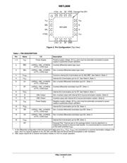
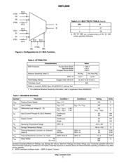
Figure 1. Simplified Logic Diagram
D0
Q
SEL
VTD0
Q
SEL
VTD0
50 W
50 W
D0
D1
VTD1
VTD1
50 W
50 W
D1
50 W
50 W
VTSEL
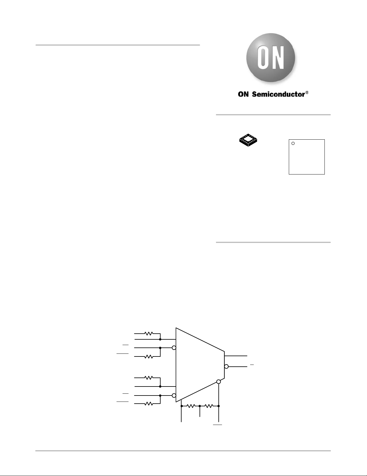
http://onsemi.com
QFN16
MN SUFFIX
CASE 485G
MARKING
DIAGRAM*
*For additional marking information, refer to
Application Note AND8002/D.
A = Assembly Location
L = Wafer Lot
Y = Year
W = Work Week
G = Pb−Free Package
16
NB7L
86M
ALYWG
G
1
See detailed ordering and shipping information in the package
dimensions section on page 11 of this data sheet.
ORDERING INFORMATION
1
器件 Datasheet 文档搜索
AiEMA 数据库涵盖高达 72,405,303 个元件的数据手册,每天更新 5,000 多个 PDF 文件
