Datasheet 搜索 > MOS管 > ON Semiconductor(安森美) > NTD3055L104 数据手册 > NTD3055L104 开发手册 1/9 页

¥ 1.599
NTD3055L104 开发手册 - ON Semiconductor(安森美)
制造商:
ON Semiconductor(安森美)
分类:
MOS管
封装:
TO-252-3
描述:
60V,12A,逻辑电平N沟道功率MOSFET
Pictures:
3D模型
符号图
焊盘图
引脚图
产品图
页面导航:
引脚图在P1Hot
典型应用电路图在P1
封装尺寸在P8P9
焊盘布局在P8
型号编码规则在P1P7P9
标记信息在P1P9
封装信息在P7
技术参数、封装参数在P7
应用领域在P1
电气规格在P2
型号编号列表在P1
导航目录
NTD3055L104数据手册
Page:
of 9 Go
若手册格式错乱,请下载阅览PDF原文件
© Semiconductor Components Industries, LLC, 2014
July, 2014 − Rev. 9
1 Publication Order Number:
NTD3055L104/D
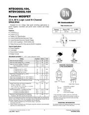
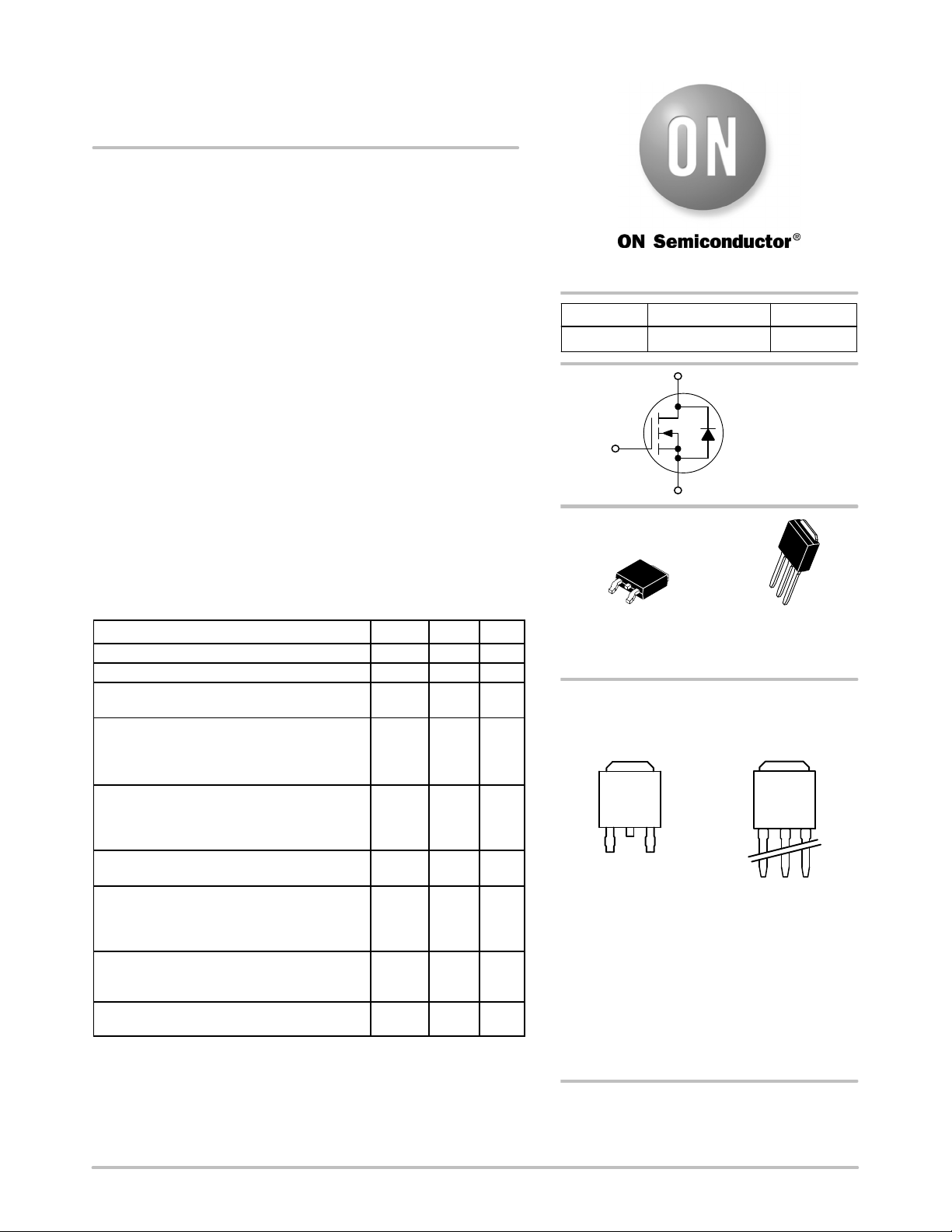
NTD3055L104,
NTDV3055L104
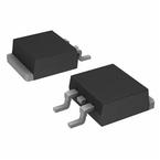
Power MOSFET
12 A, 60 V, Logic Level N−Channel
DPAK/IPAK
Designed for low voltage, high speed switching applications in
power supplies, converters and power motor controls and bridge
circuits.
Features
• Lower R
DS(on)
• Lower V
DS(on)
• Tighter V
SD
Specification
• Lower Diode Reverse Recovery Time
• Lower Reverse Recovery Stored Charge
• AEC Q101 Qualified − NTDV3055L104
• These Devices are Pb−Free and are RoHS Compliant
Typical Applications
• Power Supplies
• Converters
• Power Motor Controls
• Bridge Circuits
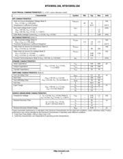
MAXIMUM RATINGS (T
J
= 25°C unless otherwise noted)
Rating
Symbol Value Unit
Drain−to−Source Voltage V
DSS
60 Vdc
Drain−to−Gate Voltage (R
GS
= 10 MW)
V
DGR
60 Vdc
Gate−to−Source Voltage, Continuous
− Non−Repetitive (t
p
v10 ms)
V
GS
V
GS
"15
"20
Vdc
Drain Current
− Continuous @ T
A
= 25°C
− Continuous @ T
A
= 100°C
− Single Pulse (t
p
v10 ms)
I
D
I
D
I
DM
12
10
45
Adc
Apk
Total Power Dissipation @ T
A
= 25°C
Derate above 25°C
Total Power Dissipation @ T
A
= 25°C (Note 1)
Total Power Dissipation @ T
A
= 25°C (Note 2)
P
D
48
0.32
2.1
1.5
W
W/°C
W
W
Operating and Storage Temperature Range T
J
, T
stg
−55 to
+175
°C
Single Pulse Drain−to−Source Avalanche
Energy − Starting T
J
= 25°C
(V
DD
= 25 Vdc, V
GS
= 5.0 Vdc, L = 1.0 mH
I
L(pk)
= 11 A, V
DS
= 60 Vdc)
E
AS
61 mJ
Thermal Resistance, − Junction−to−Case
− Junction−to−Ambient (Note 1)
− Junction−to−Ambient (Note 2)
R
q
JC
R
q
JA
R
q
JA
3.13
71.4
100
°C/W
Maximum Lead Temperature for Soldering
Purposes, 1/8″ from case for 10 seconds
T
L
260 °C
Stresses exceeding those listed in the Maximum Ratings table may damage the
device. If any of these limits are exceeded, device functionality should not be
assumed, damage may occur and reliability may be affected.
1. When surface mounted to an FR4 board using 1″ pad size,
(Cu Area 1.127 in
2
).
2. When surface mounted to an FR4 board using the minimum recommended
pad size, (Cu Area 0.412 in
2
).
N−Channel
D
S
G
60 V
104 mW
R
DS(on)
TYP
12 A
I
D
MAXV
(BR)DSS
See detailed ordering and shipping information in the package
dimensions section on page 7 of this data sheet.
ORDERING INFORMATION
1
Gate
3
Source
2
Drain
4
Drain
DPAK
CASE 369C
STYLE 2
MARKING DIAGRAMS
& PIN ASSIGNMENTS
1
2
3
4
1
Gate
3
Source
2
Drain
4
Drain
IPAK
CASE 369D
STYLE 2
1
2
3
4
AYWW
55L
104G
AYWw
55L
104G
A = Assembly Location*
55L104 = Device Code
Y = Year
WW = Work Week
G = Pb−Free Package
http://onsemi.com
* The Assembly Location code (A) is front side
optional. In cases where the Assembly Location is
stamped in the package, the front side assembly
code may be blank.
器件 Datasheet 文档搜索
AiEMA 数据库涵盖高达 72,405,303 个元件的数据手册,每天更新 5,000 多个 PDF 文件
