Datasheet 搜索 > ADI(亚德诺) > OP296 数据手册 > OP296 开发手册 1/28 页


¥ 0
OP296 开发手册 - ADI(亚德诺)
制造商:
ADI(亚德诺)
描述:
运算放大器选型指南 Operational Amplifiers Selection Guide
Pictures:
3D模型
符号图
焊盘图
引脚图
产品图
OP296数据手册
Page:
of 28 Go
若手册格式错乱,请下载阅览PDF原文件
AN-649
APPLICATION NOTE
One Technology Way • P.O. Box 9106 • Norwood, MA 02062-9106 • Tel: 781/329-4700 • Fax: 781/326-8703 • www.analog.com
Using the Analog Devices Active Filter Design Tool
By Hank Zumbahlen
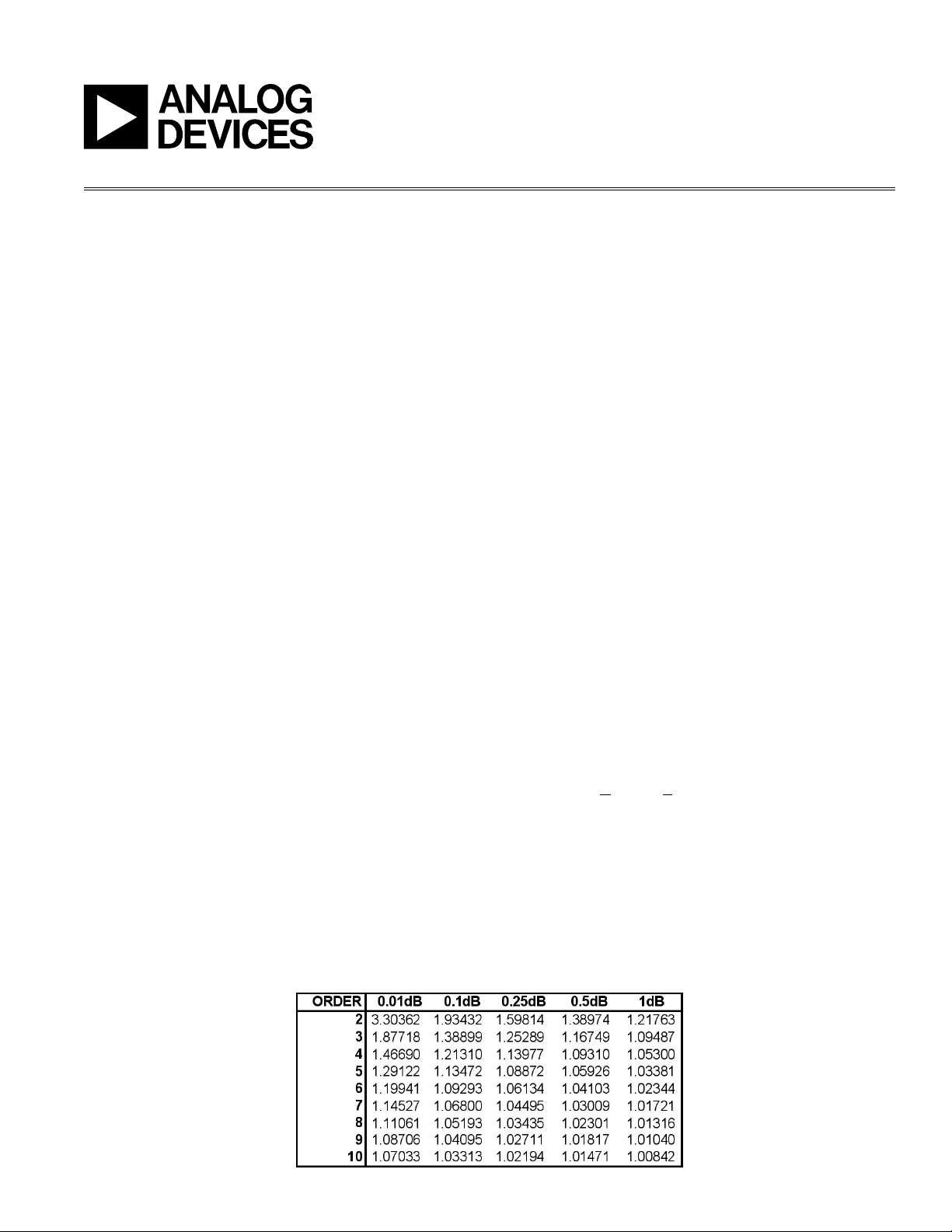
Table I. Chebyshev Cutoff Frequency to –3 dB Frequency
INTRODUCTION
The Analog Devices Active Filter Design Tool assists the
engineer in designing all-pole active lters.
The lter design process consists of two steps. In Step 1,
the response of the lter is determined, meaning the
attenuation and/or phase response of the lter is dened.
In Step 2, the topology of the lter—how it is built—is
dened. This application note is intended to help in Step 1.
Several different standard responses are discussed, and
their attenuation, group delay, step response, and impulse
response are presented. The lter tool is then employed
to design the lter. An example is provided.
STANDARD RESPONSES
Many transfer functions may be used to satisfy the atten-
uation and/or phase requirements of a particular lter. The
one that is selected will depend on the particular system.
The importance of frequency domain response versus
time domain response must be determined. Also, both
of these might be traded off against lter complexity, and
therefore cost.
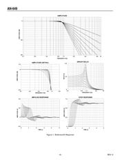
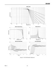
BUTTERWORTH FILTER
The Butterworth lter is the best compromise between
attenuation and phase response. It has no ripple in the
pass band or the stop band; because of this, it is some-
times called a maximally at lter. The Butterworth lter
achieves its atness at the expense of a relatively wide
transition region from pass band to stop band, with aver-
age transient characteristics.
The values of the elements of the Butterworth lter are
more practical and less critical than many other lter
types. The frequency response, group delay, impulse
response, and step response are shown in Figure 1. The
pole locations and corresponding
o
and terms are
tabulated in Table II.
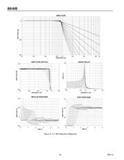
CHEBYSHEV FILTER
The Chebyshev (or Chevyshev, Tschebychev, Tsche -
byscheff, or Tchevysheff, depending on the translation
from Russian) lter has a smaller transition region than
the same-order Butterworth lter, at the expense of
ripples in its pass band. This lter gets its name from
the Chebyshev criterion, which minimizes the height of
the maximum ripple.
Chebyshev lters have 0 dB relative attenuation at dc.
Odd-order lters have an attenuation band that extends
from 0 dB to the ripple value. Even-order lters have
a gain equal to the pass-band ripple. The number of
cycles of ripple in the pass band is equal to the order of
the lter.
The Chebyshev lters are typically normalized so that the
edge of the ripple band is at
o
= 1.
The 3 dB bandwidth is given by
A
n
dB3
1
1 1
=
cosh
–
ε
(1)
This is tabulated in Table I.
Figures 2 through 6 show the frequency response, group
delay, impulse response, and step response for the various
Chebyshev lters. The pole locations and corresponding
o
and
terms are tabulated in Tables III through VII.
REV. 0
器件 Datasheet 文档搜索
AiEMA 数据库涵盖高达 72,405,303 个元件的数据手册,每天更新 5,000 多个 PDF 文件
