Datasheet 搜索 > 微控制器 > Microchip(微芯) > PIC18F26K20-I/SO 数据手册 > PIC18F26K20-I/SO 开发手册 1/18 页
 器件3D模型
¥ 20.522
PIC18F26K20-I/SO 开发手册 - Microchip(微芯)
制造商:
Microchip(微芯)
分类:
微控制器
封装:
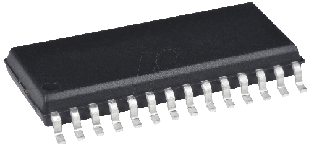
SOIC-28
描述:
MICROCHIP PIC18F26K20-I/SO 微控制器, 8位, 闪存, AEC-Q100, PIC18FxxKxx, 64 MHz, 64 KB, 3.84 KB, 28 引脚, SOIC
Pictures:
3D模型
符号图
焊盘图
引脚图
产品图
页面导航:
应用领域在P1P5P15
导航目录
PIC18F26K20-I/SO数据手册
Page:
of 18 Go
若手册格式错乱,请下载阅览PDF原文件
© 2011 Microchip Technology Inc. DS01095D-page 1
AN1095
INTRODUCTION
Microchip Technology Inc., has expanded its product
portfolio to include a wide variety of cost-effective PIC
®
Microcontrollers (MCUs) without an internal data
EEPROM.
Many applications store nonvolatile information in the
Flash program memory using table read and write
operations. Applications that need to frequently update
this data may have greater endurance requirements
than the specified Flash endurance for the MCUs/
Digital Signal Controllers (DSCs) devices.
The alternate solution of using an external, serial
EEPROM device may not be appropriate for
cost-sensitive or pin-constrained applications.
This application note presents a third alternative that
addresses these issues. This algorithm features an
interface similar to an internal data EEPROM which
uses available program memory and can improve
endurance by a factor as high as 500.
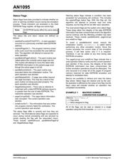
Definition of Terms
Page – The minimum amount of program memory
affected by an erase operation.
Row – The maximum amount of program memory
affected by a programming operation.
Erase/Write Cycle – The number of erase and write
operation pairs.
Endurance – A specification indicating the maximum
number of erase/write cycles and associated conditions.
Retention – A specification indicating the minimum time
and associated conditions for the retention of data in
Flash program memory.
Effective Endurance – The improved endurance of the
emulated data EEPROM as a result of using an
efficient programming algorithm.
Current (Active) Page – A page in program memory
that is being written and read by the data EEPROM
emulation algorithm.
Packed Page – The new current page after the pack
routine is complete.
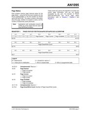
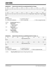
Page Status – Program memory locations at the
beginning of the current page that stores data
EEPROM emulation status. The PIC18 implementation
uses two locations and PIC24/dsPIC33F/dsPIC33E
uses one location.
THEORY OF OPERATION
The algorithm in this application note supports
selectable, multiple emulated data EEPROMs with a
total size of up to multiples of 255 locations, with a
single address space, ranging from 0 to the total size of
the emulated data EEPROMs minus one (see the
below note).
For example, if the implemented size of the data
EEPROM is five, and two data EEPROMs are used,
only the addresses in the range, 0 to 9, are available.
PIC18 implementation supports 8-bit data and multiple
EEPROM banks; PIC24/dsPIC33F/dsPIC33E
implementation supports 16-bit data and multiple
EEPROM banks. Due to architectural differences of the
program memory, the emulated data EEPROM
information is stored differently for 8-bit and 16-bit
implementations. For these formats, refer to Table 1
and Ta b l e 2.
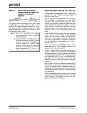
TABLE 1: PIC18 DATA EEPROM
INFORMATION FORMAT IN
PROGRAM MEMORY
Author: David Otten, Stephen Cowden and
Pradeep Budagutta
Microchip Technology Inc.
Note: To use this solution, the device must have
word write capability. Refer to the specific
device data sheet to verify the availability
of this feature.
Note: The PIC18 and PIC24/dsPIC33F/
dsPIC33E implementations support
multiple EEPROM banks. Each EEPROM
can have a maximum of 255 addresses.
Therefore, the total addresses are from
0 to N x 255 - 1, where N = the number of
EEPROM banks.
Bits 15-8 Bits 7-0
Data EE Data
Data EE Address
Emulating Data EEPROM for PIC18 and PIC24
Microcontrollers and dsPIC
®
Digital Signal Controllers
器件 Datasheet 文档搜索
AiEMA 数据库涵盖高达 72,405,303 个元件的数据手册,每天更新 5,000 多个 PDF 文件
