Datasheet 搜索 > 逻辑控制器 > TI(德州仪器) > TXS0108EPWRG4 数据手册 > TXS0108EPWRG4 开发手册 4/31 页
 器件3D模型
¥ 0.477
TXS0108EPWRG4 开发手册 - TI(德州仪器)
制造商:
TI(德州仪器)
分类:
逻辑控制器
封装:
TSSOP-20
描述:
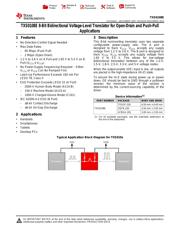
8位双向电压电平转换为漏极开路和推挽应用 8-BIT BIDIRECTIONAL VOLTAGE-LEVEL TRANSLATOR FOR OPEN-DRAIN AND PUSH-PULL APPLICATIONS
Pictures:
3D模型
符号图
焊盘图
引脚图
产品图
页面导航:
引脚图在P3P4Hot
典型应用电路图在P1P17
原理图在P1P14
封装尺寸在P21P23P24
标记信息在P21
封装信息在P20P21P22P23P24
技术参数、封装参数在P4
应用领域在P1P31
电气规格在P6
导航目录
TXS0108EPWRG4数据手册
Page:
of 31 Go
若手册格式错乱,请下载阅览PDF原文件
TXS0108E
SCES642C –DECEMBER 2007–REVISED DECEMBER 2014
www.ti.com
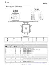
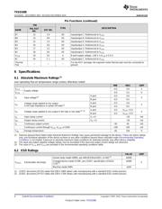
Pin Functions (continued)
PIN
TYPE DESCRIPTION
PW, RGY
NAME ZXY NO.
NO.
B7 13 C4 I/O Input/output 7. Referenced to V
CCB
B6 14 D4 I/O Input/output 6. Referenced to V
CCB
B5 15 C3 I/O Input/output 5. Referenced to V
CCB
B4 16 D3 I/O Input/output 4. Referenced to V
CCB
B3 17 C2 I/O Input/output 3. Referenced to V
CCB
B2 18 D2 I/O Input/output 2. Referenced to V
CCB
V
CCB
19 D1 S B-port supply voltage. 1.65 V ≤ V
CCB
≤ 5.5 V.
B1 20 C 1 I/O Input/output 1. Referenced to V
CCB
Thermal For the RGY package, the exposed center thermal pad must be connected to
— — —
Pad ground
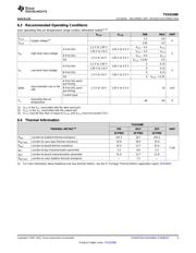
6 Specifications
6.1 Absolute Maximum Ratings
(1)
over operating free-air temperature range (unless otherwise noted)
MIN MAX UNIT
V
CCA
–0.5 4.6 V
Supply voltage
V
CCB
–0.5 5.5 V
A port –0.5 4.6
V
I
Input voltage
(2)
V
B port –0.5 6.5
A port –0.5 4.6
Voltage range applied to any output
V
O
V
in the high-impedance or power-off state
(2)
B port –0.5 6.5
A port –0.5 V
CCA
+ 0.5
V
O
Voltage range applied to any output in the high or low state
(2) (3)
V
B port –0.5 V
CCB
+ 0.5
I
IK
Input clamp current V
I
< 0 –50 mA
I
OK
Output clamp current V
O
< 0 –50 mA
I
O
Continuous output current –50 50 mA
Continuous current through V
CCA
, V
CCB
, or GND –100 100 mA
T
stg
Storage temperature –65 150 °C
(1) Stresses beyond those listed under Absolute Maximum Ratings may cause permanent damage to the device. These are stress ratings
only, and functional operation of the device at these or any other conditions beyond those indicated under Recommended Operating
Conditions is not implied. Exposure to absolute-maximum-rated conditions for extended periods may affect device reliability.
(2) The input and output negative-voltage ratings may be exceeded if the input and output current ratings are observed.
(3) The value of V
CCA
and V
CCB
are provided in the recommended operating conditions table.
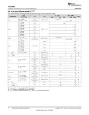
6.2 ESD Ratings
VALUE UNIT
Human body model (HBM), per ANSI/ESDA/JEDEC JS-001
(1)
±2000
Charged-device model (CDM), per JEDEC specification JESD22- ±1000
V
(ESD)
Electrostatic discharge V
C101
(2)
Machine model (MM) ±150
(1) JEDEC document JEP155 states that 500-V HBM allows safe manufacturing with a standard ESD control process.
(2) JEDEC document JEP157 states that 250-V CDM allows safe manufacturing with a standard ESD control process.
4 Submit Documentation Feedback Copyright © 2007–2014, Texas Instruments Incorporated
Product Folder Links: TXS0108E
器件 Datasheet 文档搜索
AiEMA 数据库涵盖高达 72,405,303 个元件的数据手册,每天更新 5,000 多个 PDF 文件
