Datasheet 搜索 > 齐纳二极管 > Micro Commercial Components(美微科) > 1N5361B-TP 数据手册 > 1N5361B-TP 数据手册 3/6 页

¥ 0.741
1N5361B-TP 数据手册 - Micro Commercial Components(美微科)
制造商:
Micro Commercial Components(美微科)
分类:
齐纳二极管
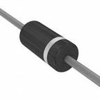
封装:
DO-204AC
Pictures:
3D模型
符号图
焊盘图
引脚图
产品图
页面导航:
型号编码规则在P6
标记信息在P1
封装信息在P1
电气规格在P2


导航目录
1N5361B-TP数据手册
Page:
of 6 Go
若手册格式错乱,请下载阅览PDF原文件

3. SURGE CURRENT (Ir) - Surge current is specified as the maximum allowable peak, non-recurrent square-wave
current with a pulse width, PW, of 8.3 ms. The data given in Figure 5 may be used to find the maximum surge
current for a quare wave of any pulse width between 1 ms and 1000ms by plotting the applicable points on
logarithmic paper. Examples of this, using the 6.8v , is shown in Figure 6. Mounting
contact located as specified in Note 3. (T
A
=25 ).
4. VOLTAGE REGULATION (Vz) - Test conditions for voltage regulation are as follows: Vz measurements are made
at 10% and then at 50% of the Iz max value listed in the electrical characteristics table. The test currents are the
same for the 5% and 10% tolerance devices. The test current time druation for each Vz measurement is 40+/- 10 ms.
(T
A
=25C ). Mounting contact located as specified in Note2.
5. MAXIMUM REGULATOR CURRENT (I
ZM
) - The maximum current shown is based on the maximum voltage of a
5% type unit. Therefore, it applies only to the B-suffix device. The actual I
ZM
for any device may not exceed the
value of 5 watts divided by the actual Vz of the device. T
L
=75Cat maximum from the device body.
APPLICATION NOTE:
1N53
3
8B
T
H
RU 1N
5
3
6
9B
MCC
Revision: A 2011/01/01
TM
Micro Commercial Components
ć
www.mccsemi.com
3 of 6
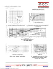
Since the actual voltage available from a given Zener
diode is temperature dependent, it is necessary to determine
junction temperature under any set of operating conditions
in order to calculate its value. The following procedure is
recommended:
Lead Temperature, T
L
, should be determined from:
T
L
= q
LA
P
D
+ T
A
q
LA
is the lead‐to‐ambient thermal resistance and P
D
is the
power dissipation.
Junction Temperature, T
J
, may be found from:
T
J
= T
L
+ DT
JL
DT
JL
is the increase in junction temperature above the lead
temperature and may be found from Figure 4 for a train of
power pulses or from Figure 1 for dc power.
DT
JL
= q
JL
P
D
For worst‐case design, using expected limits of I
Z
, limits
of P
D
and the extremes of T
J
(DT
J
) may be estimated.
Changes in voltage, V
Z
, can then be found from:
DV = q
VZ
DT
J
q
VZ
, the Zener voltage temperature coefficient, is found
from Figures 2 and 3.
Under high power‐pulse operation, the Zener voltage will
vary with time and may also be affected significantly by the
zener resistance. For best regulation, keep current
excursions as low as possible.
Data of Figure 4 should not be used to compute surge
capability. Surge limitations are given in Figure 5. They are
lower than would be expected by considering only junction
temperature, as current crowding effects cause temperatures
to be extremely high in small spots resulting in device
degradation should the limits of Figure 5 be exceeded.
Downloaded from Elcodis.com electronic components distributor
器件 Datasheet 文档搜索
AiEMA 数据库涵盖高达 72,405,303 个元件的数据手册,每天更新 5,000 多个 PDF 文件
