Datasheet 搜索 > 齐纳二极管 > ON Semiconductor(安森美) > 1N5388BG 数据手册 > 1N5388BG 数据手册 3/7 页

¥ 1.242
1N5388BG 数据手册 - ON Semiconductor(安森美)
制造商:
ON Semiconductor(安森美)
分类:
齐纳二极管
封装:
DO-35-2
描述:
ON SEMICONDUCTOR 1N5388BG 单管二极管 齐纳, 200 V, 5 W, 017AA, 5 %, 2 引脚, 200 °C
Pictures:
3D模型
符号图
焊盘图
引脚图
产品图
页面导航:
导航目录
1N5388BG数据手册
Page:
of 7 Go
若手册格式错乱,请下载阅览PDF原文件
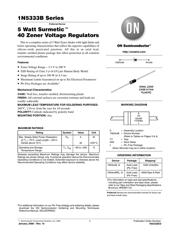
1N5333B Series
http://onsemi.com
3
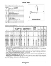
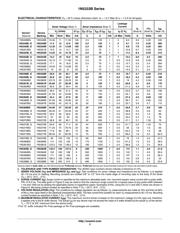
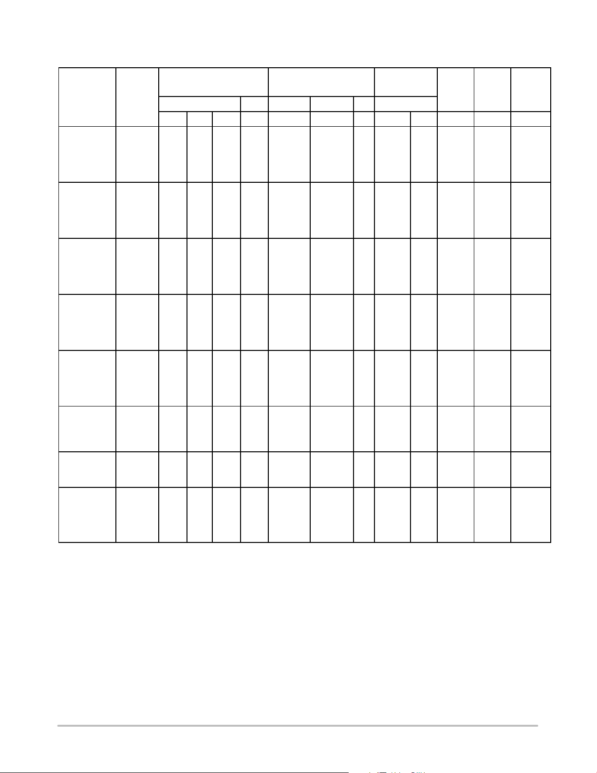
ELECTRICAL CHARACTERISTICS (T
A
= 25°C unless otherwise noted, V
F
= 1.2 V Max @ I
F
= 1.0 A for all types)
Device
†
(Note 6)
Device
Marking
Zener Voltage (Note 7) Zener Impedance (Note 7)
Leakage
Current
I
R
(Note 8)
DV
Z
(Note 9)
I
ZM
(Note 10)
V
Z
(Volts) @ I
ZT
Z
ZT
@ I
ZT
Z
ZK
@ I
ZK
I
ZK
I
R
@ V
R
Min Nom Max mA
W W
mA
mA Max
Volts A Volts mA
1N5348BG 1N5348B 10.45 11 11.55 125 2.5 125 1 5 8.4 8.0 0.25 430
1N5349B, G 1N5349B 11.4 12 12.6 100 2.5 125 1 2 9.1 7.5 0.25 395
1N5350B, G 1N5350B 12.35 13 13.65 100 2.5 100 1 1 9.9 7.0 0.25 365
1N5351BG 1N5351B 13.3 14 14.7 100 2.5 75 1 1 10.6 6.7 0.25 340
1N5352B, G 1N5352B 14.25 15 15.75 75 2.5 75 1 1 11.5 6.3 0.25 315
1N5353B, G 1N5353B 15.2 16 16.8 75 2.5 75 1 1 12.2 6.0 0.3 295
1N5354B, G 1N5354B 16.15 17 17.85 70 2.5 75 1 0.5 12.9 5.8 0.35 280
1N5355B, G 1N5355B 17.1 18 18.9 65 2.5 75 1 0.5 13.7 5.5 0.4 264
1N5356BG 1N5356B 18.05 19 19.95 65 3 75 1 0.5 14.4 5.3 0.4 250
1N5357BG 1N5357B 19 20 21 65 3 75 1 0.5 15.2 5.1 0.4 237
1N5358B, G 1N5358B 20.9 22 23.1 50 3.5 75 1 0.5 16.7 4.7 0.45 216
1N5359B, G 1N5359B 22.8 24 25.2 50 3.5 100 1 0.5 18.2 4.4 0.55 198
1N5360BG 1N5360B 23.75 25 26.25 50 4 110 1 0.5 19 4.3 0.55 190
1N5361B, G 1N5361B 25.65 27 28.35 50 5 120 1 0.5 20.6 4.1 0.6 176
1N5362BG 1N5362B 26.6 28 29.4 50 6 130 1 0.5 21.2 3.9 0.6 170
1N5363BG 1N5363B 28.5 30 31.5 40 8 140 1 0.5 22.8 3.7 0.6 158
1N5364BG 1N5364B 31.35 33 34.65 40 10 150 1 0.5 25.1 3.5 0.6 144
1N5365B, G 1N5365B 34.2 36 37.8 30 11 160 1 0.5 27.4 3.5 0.65 132
1N5366B, G 1N5366B 37.05 39 40.95 30 14 170 1 0.5 29.7 3.1 0.65 122
1N5367BG 1N5367B 40.85 43 45.15 30 20 190 1 0.5 32.7 2.8 0.7 110
1N5368BG 1N5368B 44.65 47 49.35 25 25 210 1 0.5 35.8 2.7 0.8 100
1N5369B, G 1N5369B 48.45 51 53.55 25 27 230 1 0.5 38.8 2.5 0.9 93
1N5370B, G 1N5370B 53.2 56 58.8 20 35 280 1 0.5 42.6 2.3 1.0 86
1N5371BG 1N5371B 57 60 63 20 40 350 1 0.5 45.5 2.2 1.2 79
1N5372BG 1N5372B 58.9 62 65.1 20 42 400 1 0.5 47.1 2.1 1.35 76
1N5373B, G 1N5373B 64.6 68 71.4 20 44 500 1 0.5 51.7 2.0 1.52 70
1N5374BG 1N5374B 71.25 75 78.75 20 45 620 1 0.5 56 1.9 1.6 63
1N5375BG 1N5375B 77.9 82 86.1 15 65 720 1 0.5 62.2 1.8 1.8 58
1N5377BG 1N5377B 86.45 91 95.55 15 75 760 1 0.5 69.2 1.6 2.2 52.5
1N5378B, G 1N5378B 95 100 105 12 90 800 1 0.5 76 1.5 2.5 47.5
1N5380BG 1N5380B 114 120 126 10 170 1150 1 0.5 91.2 1.3 2.5 39.5
1N5381BG 1N5381B 123.5 130 136.5 10 190 1250 1 0.5 98.8 1.2 2.5 36.6
1N5383B, G 1N5383B 142.5 150 157.5 8 330 1500 1 0.5 114 1.1 3.0 31.6
1N5384BG 1N5384B 152 160 168 8 350 1650 1 0.5 122 1.1 3.0 29.4
1N5386BG 1N5386B 171 180 189 5 430 1750 1 0.5 137 1.0 4.0 26.4
1N5387BG 1N5387B 180.5 190 199.5 5 450 1850 1 0.5 144 0.9 5.0 25
1N5388B, G 1N5388B 190 200 210 5 480 1850 1 0.5 152 0.9 5.0 23.6
Devices listed in bold, italic are ON Semiconductor Preferred devices. Preferred devices are recommended choices for future use and best overall value.
6. TOLERANCE AND TYPE NUMBER DESIGNATION: The JEDEC type numbers shown indicate a tolerance of ±5%.
7. ZENER VOLTAGE (V
Z
) and IMPEDANCE (I
ZT
and I
ZK
): Test conditions for zener voltage and impedance are as follows: I
Z
is applied
40 ±10 ms prior to reading. Mounting contacts are located 3/8″ to 1/2″ from the inside edge of mounting clips to the body of the diode
(T
A
= 25°C +8°C, -2°C).
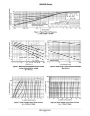
8. SURGE CURRENT (I
R
): Surge current is specified as the maximum allowable peak, non-recurrent square-wave current with a pulse width,
PW, of 8.3 ms. The data given in Figure 5 may be used to find the maximum surge current for a square wave of any pulse width between
1 ms and 1000 ms by plotting the applicable points on logarithmic paper. Examples of this, using the 3.3 V and 200 V zener are shown in
Figure 6. Mounting contact located as specified in Note 7 (T
A
= 25°C +8°C, -2°C).
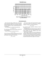
9. VOLTAGE REGULATION (DV
Z
): The conditions for voltage regulation are as follows: V
Z
measurements are made at 10% and then at 50%
of the I
Z
max value listed in the electrical characteristics table. The test current time duration for each V
Z
measurement is 40 ±10 ms. Mounting
contact located as specified in Note 7 (T
A
= 25°C +8°C, -2°C).
10.MAXIMUM REGULATOR CURRENT (I
ZM
): The maximum current shown is based on the maximum voltage of a 5% type unit, therefore,
it applies only to the B-suffix device. The actual I
ZM
for any device may not exceed the value of 5 watts divided by the actual V
Z
of the device.
T
L
= 75°C at 3/8″ maximum from the device body.
†The “G'' suffix indicates Pb-Free package or Pb-Free packages are available.
器件 Datasheet 文档搜索
AiEMA 数据库涵盖高达 72,405,303 个元件的数据手册,每天更新 5,000 多个 PDF 文件
