Datasheet 搜索 > EEPROM芯片 > Microchip(微芯) > 24LC65-I/P 数据手册 > 24LC65-I/P 数据手册 3/24 页
 器件3D模型
¥ 0.709
24LC65-I/P 数据手册 - Microchip(微芯)
制造商:
Microchip(微芯)
分类:
EEPROM芯片
封装:
DIP-8
描述:
MICROCHIP 24LC65-I/P EEPROM, Smart Serial™, AEC-Q100, 64 Kbit, 8K x 8位, 400 kHz, I2C, DIP, 8 引脚
Pictures:
3D模型
符号图
焊盘图
引脚图
产品图
页面导航:
导航目录
24LC65-I/P数据手册
Page:
of 24 Go
若手册格式错乱,请下载阅览PDF原文件
© 2008 Microchip Technology Inc. DS21073K-page 3
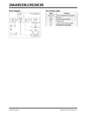
24AA65/24LC65/24C65
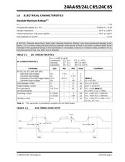
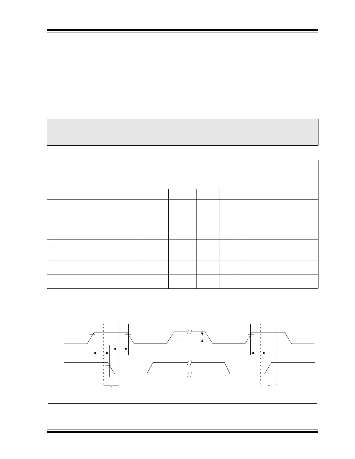
1.0 ELECTRICAL CHARACTERISTICS
Absolute Maximum Ratings
(†)
VCC.............................................................................................................................................................................7.0V
All inputs and outputs w.r.t. V
SS ..........................................................................................................-0.6V to VCC +1.0V
Storage temperature ...............................................................................................................................-65°C to +150°C
Ambient temperature with power applied................................................................................................-40°C to +125°C
ESD protection on all pins......................................................................................................................................................≥ 4 kV
TABLE 1-1: DC CHARACTERISTICS
FIGURE 1-1: BUS TIMING START/STOP
† NOTICE: Stresses above those listed under “Absolute Maximum Ratings” may cause permanent damage to the
device. This is a stress rating only and functional operation of the device at those or any other conditions above those
indicated in the operational listings of this specification is not implied. Exposure to maximum rating conditions for an
extended period of time may affect device reliability.
DC CHARACTERISTICS
V
CC = +1.8V to +6.0V
Commercial (C): T
A =0°C to +70°C
Industrial (I): T
A =-40°C to +85°C
Automotive (E): T
A =-40°C to +125°C
Parameter Sym Min Max Units Conditions
A0, A1, A2, SCL and SDA pins:
High-level input voltage
Low-level input voltage
Hysteresis of Schmitt Trigger inputs
Low-level output voltage
V
IH
VIL
VHYS
VOL
.7 VCC
—
.05 V
CC
—
—
.3 VCC
—
.40
V
V
V
V
(Note 1)
I
OL = 3.0 mA
Input leakage current I
LI — ±1 μAVIN = .1V to VCC
Output leakage current ILO — ±1 μAVOUT = .1V to VCC
Pin capacitance
(all inputs/outputs)
CIN, COUT —10pFVCC = 5.0V (Note 1)
T
A = 25°C, FCLK = 1 MHz
Operating current ICC Write
I
CC Read
—
—
3
150
mA
μA
V
CC = 6.0V, SCL = 400 kHz
V
CC = 6.0V, SCL = 400 kHz
Standby current ICCS —5μAVCC = 5.0V, SCL = SDA = VCC
A0, A1, A2 = VSS
Note 1: This parameter is periodically sampled and not 100% tested.
TSU:STA
THD:STA
VHYS
TSU:STO
Start Stop
SCL
SDA
器件 Datasheet 文档搜索
AiEMA 数据库涵盖高达 72,405,303 个元件的数据手册,每天更新 5,000 多个 PDF 文件
