Datasheet 搜索 > Skyworks Solutions > 510ABA125M000AAGR 数据手册 > 510ABA125M000AAGR 数据手册 26/31 页


¥ 0
510ABA125M000AAGR 数据手册 - Skyworks Solutions
制造商:
Skyworks Solutions
Pictures:
3D模型
符号图
焊盘图
引脚图
产品图
页面导航:
引脚图在P1P12Hot
典型应用电路图在P31
原理图在P1
封装尺寸在P9P16P18P20P22P24P27
型号编码规则在P1P14
封装信息在P14
焊接温度在P11
技术参数、封装参数在P3P10
应用领域在P1
电气规格在P3
导航目录
510ABA125M000AAGR数据手册
Page:
of 31 Go
若手册格式错乱,请下载阅览PDF原文件
Si510/511
26 Rev. 1.4
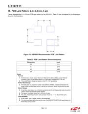
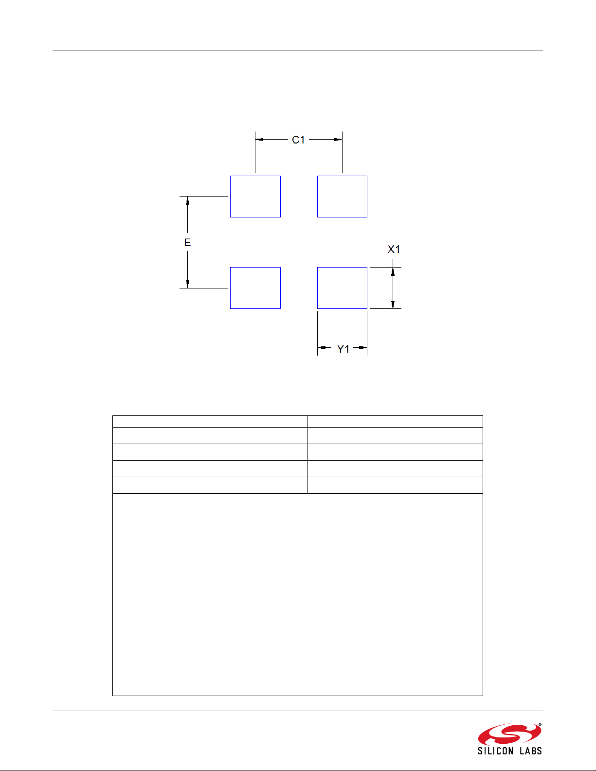
15. PCB Land Pattern: 2.5 x 3.2 mm, 4-pin
Figure illustrates the 2.5 x 3.2 mm PCB land pattern for the Si510/511. Table 23 lists the values for the dimensions
shown in the illustration.
Figure 13. Si510/511 Recommended PCB Land Pattern
Table 23. PCB Land Pattern Dimensions (mm)
Dimension (mm)
C1 2.0
E2.10
X1 0.95
Y1 1.15
Notes:
General
1. All dimensions shown are at Maximum Material Condition (MMC). Least Material
Condition (LMC) is calculated based on a Fabrication Allowance of 0.05 mm.
2. This Land Pattern Design is based on the IPC-7351 guidelines.
Solder Mask Design
3. All metal pads are to be non-solder mask defined (NSMD). Clearance between the
solder mask and the metal pad is to be 60 µm minimum, all the way around the pad.
Stencil Design
4. A stainless steel, laser-cut and electro-polished stencil with trapezoidal walls should be
used to assure good solder paste release.
5. The stencil thickness should be 0.125 mm (5 mils).
6. The ratio of stencil aperture to land pad size should be 1:1 for all perimeter pins.
Card Assembly
7. A No-Clean, Type-3 solder paste is recommended.
8. The recommended card reflow profile is per the JEDEC/IPC J-STD-020 specification for
Small Body Components.
器件 Datasheet 文档搜索
AiEMA 数据库涵盖高达 72,405,303 个元件的数据手册,每天更新 5,000 多个 PDF 文件
