Datasheet 搜索 > CPLD芯片 > Altera(阿尔特拉) > 5M160ZE64C5N 数据手册 > 5M160ZE64C5N 数据手册 13/167 页

¥ 19.99
5M160ZE64C5N 数据手册 - Altera(阿尔特拉)
制造商:
Altera(阿尔特拉)
分类:
CPLD芯片
封装:
QFP-64
描述:
ALTERA 5M160ZE64C5N 可编程逻辑芯片, CPLD, MAX V系列, 160 LE, 64EQFP
Pictures:
3D模型
符号图
焊盘图
引脚图
产品图
页面导航:
引脚图在P118P128P140P150Hot
典型应用电路图在P13P20P21P22P23P24P25P128
原理图在P14
型号编码规则在P9
功能描述在P13P14P15P105P107P108P109P110P111
技术参数、封装参数在P44P49P51P53P54P55P56P58P59P60P61P62
电气规格在P44P49P51P52
型号编号列表在P49
导航目录
5M160ZE64C5N数据手册
Page:
of 167 Go
若手册格式错乱,请下载阅览PDF原文件

MAX V Device Handbook
December 2010
MV51002-1.0
Subscribe
© 2010 Altera Corporation. All rights reserved. ALTERA, ARRIA, CYCLONE, HARDCOPY, MAX, MEGACORE, NIOS, QUARTUS and STRATIX are Reg. U.S. Pat. & Tm. Off.
and/or trademarks of Altera Corporation in the U.S. and other countries. All other trademarks and service marks are the property of their respective holders as described at
www.altera.com/common/legal.html. Altera warrants performance of its semiconductor products to current specifications in accordance with Altera’s standard warranty, but
reserves the right to make changes to any products and services at any time without notice. Altera assumes no responsibility or liability arising out of the application or use of any
information, product, or service described herein except as expressly agreed to in writing by Altera. Altera customers are advised to obtain the latest version of device
specifications before relying on any published information and before placing orders for products or services.
2. MAX V Architecture
This chapter describes the architecture of the MAX
®
V device and contains the
following sections:
■ “Functional Description” on page 2–1
■ “Logic Array Blocks” on page 2–4
■ “Logic Elements” on page 2–8
■ “MultiTrack Interconnect” on page 2–14
■ “Global Signals” on page 2–19
■ “User Flash Memory Block” on page 2–21
■ “Internal Oscillator” on page 2–22
■ “Core Voltage” on page 2–25
■ “I/O Structure” on page 2–26
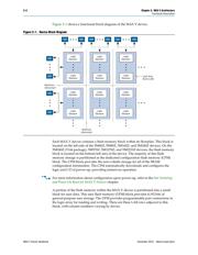
Functional Description
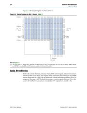
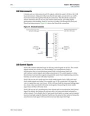
MAX V devices contain a two-dimensional row- and column-based architecture to
implement custom logic. Row and column interconnects provide signal interconnects
between the logic array blocks (LABs).
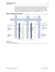
Each LAB in the logic array contains 10 logic elements (LEs). An LE is a small unit of
logic that provides efficient implementation of user logic functions. LABs are grouped
into rows and columns across the device. The MultiTrack interconnect provides fast
granular timing delays between LABs. The fast routing between LEs provides
minimum timing delay for added levels of logic versus globally routed interconnect
structures.
The I/O elements (IOEs) located after the LAB rows and columns around the
periphery of the MAX V device feeds the I/O pins. Each IOE contains a bidirectional
I/O buffer with several advanced features. I/O pins support Schmitt trigger inputs
and various single-ended standards, such as 33-MHz, 32-bit PCI™, and LVTTL.
MAX V devices provide a global clock network. The global clock network consists of
four global clock lines that drive throughout the entire device, providing clocks for all
resources within the device. You can also use the global clock lines for control signals
such as clear, preset, or output enable.
器件 Datasheet 文档搜索
AiEMA 数据库涵盖高达 72,405,303 个元件的数据手册,每天更新 5,000 多个 PDF 文件
