Datasheet 搜索 > CPLD芯片 > Altera(阿尔特拉) > 5M160ZE64C5N 数据手册 > 5M160ZE64C5N 数据手册 150/167 页

¥ 19.99
5M160ZE64C5N 数据手册 - Altera(阿尔特拉)
制造商:
Altera(阿尔特拉)
分类:
CPLD芯片
封装:
QFP-64
描述:
ALTERA 5M160ZE64C5N 可编程逻辑芯片, CPLD, MAX V系列, 160 LE, 64EQFP
Pictures:
3D模型
符号图
焊盘图
引脚图
产品图
页面导航:
引脚图在P118P128P140P150Hot
典型应用电路图在P13P20P21P22P23P24P25P128
原理图在P14
型号编码规则在P9
功能描述在P13P14P15P105P107P108P109P110P111
技术参数、封装参数在P44P49P51P53P54P55P56P58P59P60P61P62
电气规格在P44P49P51P52
型号编号列表在P49
导航目录
5M160ZE64C5N数据手册
Page:
of 167 Go
若手册格式错乱,请下载阅览PDF原文件

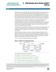
8–2 Chapter 8: JTAG Boundary-Scan Testing in MAX V Devices
IEEE Std. 1149.1 BST Architecture
MAX V Device Handbook December 2010 Altera Corporation
■ “Disabling IEEE Std. 1149.1 BST Circuitry” on page 8–15
■ “Guidelines for IEEE Std. 1149.1 Boundary-Scan Testing” on page 8–15
■ “Boundary-Scan Description Language Support” on page 8–15
In addition to BST, you can use the IEEE Std. 1149.1 controller for in-system
programming for MAX V devices. MAX V devices support IEEE 1532 programming,
which uses the IEEE Std. 1149.1 test access port (TAP) interface. However, this chapter
only describes the BST feature of the IEEE Std. 1149.1 circuitry.
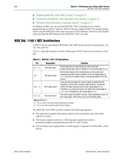
IEEE Std. 1149.1 BST Architecture
A MAX V device operating in IEEE Std. 1149.1 BST mode uses four required pins,
TDI
,
TDO
,
TMS
, and
TCK
.
Table 8–1 lists the functions of each of these pins. MAX V devices do not have a
TRST
pin.
The IEEE Std. 1149.1 BST circuitry requires the following registers:
■ The instruction register determines which action to perform and which data
register to access.
■ The bypass register (which is a 1-bit long data register) provides a
minimum-length serial path between the
TDI
and
TDO
pins.
■ The boundary-scan register that is a shift register composed of all the BSCs of the
device.
Table 8–1. IEEE Std. 1149.1 Pin Descriptions
Pin Description Function
TDI
(1) Test data input
Serial input pin for instructions as well as test and
programming data. Data is shifted in on the rising edge of
TCK
.
TDO
Test data output
Serial data output pin for instructions as well as test and
programming data. Data is shifted out on the falling edge of
TCK
. The pin is tri-stated if data is not being shifted out of the
device.
TMS
(1) Test mode select
Input pin that provides the control signal to determine the
transitions of the TAP controller state machine. Transitions
within the state machine occur at the rising edge of
TCK
.
Therefore, you must set up the
TMS
before the rising edge of
TCK
.
TMS
is evaluated on the rising edge of
TCK
.
TCK
(2) Test clock input
The clock input to the BST circuitry. Some operations occur at
the rising edge, while others occur at the falling edge.
Notes to Table 8–1:
(1) The
TDI
and
TMS
pins have internal weak pull-up resistors
(2) The
TCK
pin has an internal weak pull-down resistor
器件 Datasheet 文档搜索
AiEMA 数据库涵盖高达 72,405,303 个元件的数据手册,每天更新 5,000 多个 PDF 文件
