Datasheet 搜索 > CPLD芯片 > Altera(阿尔特拉) > 5M160ZE64C5N 数据手册 > 5M160ZE64C5N 数据手册 20/167 页

¥ 19.99
5M160ZE64C5N 数据手册 - Altera(阿尔特拉)
制造商:
Altera(阿尔特拉)
分类:
CPLD芯片
封装:
QFP-64
描述:
ALTERA 5M160ZE64C5N 可编程逻辑芯片, CPLD, MAX V系列, 160 LE, 64EQFP
Pictures:
3D模型
符号图
焊盘图
引脚图
产品图
页面导航:
引脚图在P118P128P140P150Hot
典型应用电路图在P13P20P21P22P23P24P25P128
原理图在P14
型号编码规则在P9
功能描述在P13P14P15P105P107P108P109P110P111
技术参数、封装参数在P44P49P51P53P54P55P56P58P59P60P61P62
电气规格在P44P49P51P52
型号编号列表在P49
导航目录
5M160ZE64C5N数据手册
Page:
of 167 Go
若手册格式错乱,请下载阅览PDF原文件
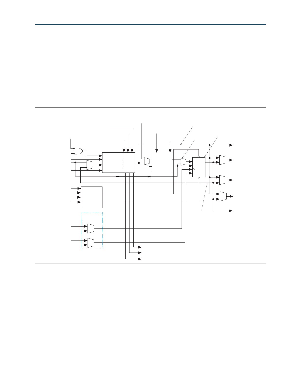
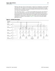
2–8 Chapter 2: MAX V Architecture
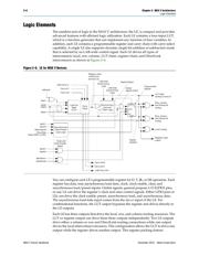
Logic Elements
MAX V Device Handbook December 2010 Altera Corporation
Logic Elements
The smallest unit of logic in the MAX V architecture, the LE, is compact and provides
advanced features with efficient logic utilization. Each LE contains a four-input LUT,
which is a function generator that can implement any function of four variables. In
addition, each LE contains a programmable register and carry chain with carry-select
capability. A single LE also supports dynamic single-bit addition or subtraction mode
that is selected by an LAB-wide control signal. Each LE drives all types of
interconnects: local, row, column, LUT chain, register chain, and DirectLink
interconnects as shown in Figure 2–6.
You can configure each LE’s programmable register for D, T, JK, or SR operation. Each
register has data, true asynchronous load data, clock, clock enable, clear, and
asynchronous load/preset inputs. Global signals, general purpose I/O (GPIO) pins,
or any LE can drive the register’s clock and clear control signals. Either GPIO pins or
LEs can drive the clock enable, preset, asynchronous load, and asynchronous data.
The asynchronous load data input comes from the
data3
input of the LE. For
combinational functions, the LUT output bypasses the register and drives directly to
the LE outputs.
Each LE has three outputs that drive the local, row, and column routing resources. The
LUT or register output can drive these three outputs independently. Two LE outputs
drive either a column or row and DirectLink routing connections while one output
drives the local interconnect resources. This configuration allows the LUT to drive one
output while the register drives another output. This register packing feature
Figure 2–6. LE for MAX V Devices
labclk1
labclk2
labclr2
labpre/aload
Carry-In1
Carry-In0
LAB Carry-In
Clock and
Clock Enable
Select
LAB Carry-Out
Carry-Out1
Carry-Out0
Look-Up
Ta ble
(LUT)
Carry
Chain
Row, column,
and DirectLink
routing
Row, column,
and DirectLink
routing
Programmable
Register
PRN/ALD
CLRN
D
Q
ENA
Register Bypass
Packed
Register Select
Chip-Wide
Reset (DEV_CLRn)
labclkena1
labclkena2
Synchronous
Load and
Clear Logic
LAB-wide
Synchronous
Load
LAB-wide
Synchronous
Clear
Asynchronous
Clear/Preset/
Load Logic
data1
data2
data3
data4
LUT chain
routing to next LE
labclr1
Local routing
Register chain
output
ADATA
addnsub
Register
Feedback
Register chain
routing from
previous LE
器件 Datasheet 文档搜索
AiEMA 数据库涵盖高达 72,405,303 个元件的数据手册,每天更新 5,000 多个 PDF 文件
