Datasheet 搜索 > 光耦合器/光隔离器 > VISHAY(威世) > 6N139 数据手册 > 6N139 数据手册 2/6 页
 器件3D模型
¥ 2.876
6N139 数据手册 - VISHAY(威世)
制造商:
VISHAY(威世)
分类:
光耦合器/光隔离器
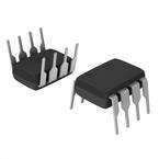
封装:
DIP-8
描述:
光耦合器,达林顿晶体管输出,Vishay Semiconductor### 光耦合器,Vishay Semiconductor
Pictures:
3D模型
符号图
焊盘图
引脚图
产品图
页面导航:
导航目录
6N139数据手册
Page:
of 6 Go
若手册格式错乱,请下载阅览PDF原文件
Document Number: 83605 For technical questions, contact: optocoupler.answers@vishay.com
www.vishay.com
Rev. 1.5, 07-May-08 185
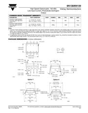
6N138/6N139
High Speed Optocoupler, 100 kBd,
Low Input Current, Photodiode Darlington
Output
Vishay Semiconductors
Notes
(1)
T
amb
= 25 °C, unless otherwise specified. Stresses in excess of the absolute maximum ratings can cause permanent damage to the device.
Functional operation of the device is not implied at these or any other conditions in excess of those given in the operational sections of this
document. Exposure to absolute maximum ratings for extended periods of the time can adversely affect reliability.
(2)
Derate linearly above 50 °C free-air temperature at a rate of 0.4 mA/°C.
(3)
Derate linearly above 50 °C free-air temperature at a rate of 0.7 mW/°C.
(4)
Derate linearly above 25 °C free-air temperature at a rate of 0.7 mA/°C.
(5)
Derate linearly above 25 °C free-air temperature at a rate of 2.0 mW/°C.
(6)
Refer to reflow profile for soldering conditions for surface mounted devices (SMD). Refer to wave profile for soldering conditions for through
hole devices (DIP).
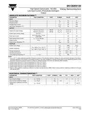
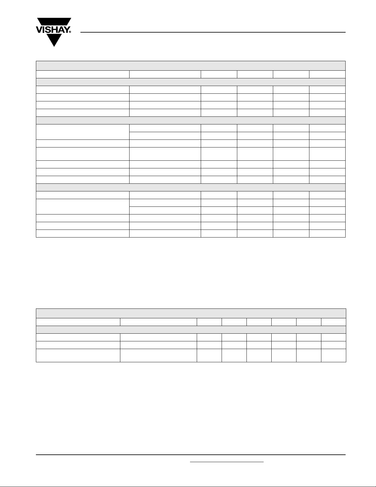
ABSOLUTE MAXIMUM RATINGS
(1)
PARAMETER TEST CONDITION PART SYMBOL VALUE UNIT
INPUT
Reverse voltage V
R
5.0 V
Forward current I
F
25 mA
Average input current I
f(avg)
20 mA
Input power dissipation
(2)(4)
P
diss
35 mW
OUTPUT
Supply and output voltage
Pin 8 to 5, pin 6 to 5 6N138 V
CC
, V
O
- 0.5 to 7.0 V
Pin 8 to 5, pin 6 to 5 6N139 V
CC
, V
O
- 0.5 to 18 V
Emitter base reverse voltage pin 5 to 7 0.5 V
Peak input current
50 % duty cycle - 1.0 ms
pulse width
40 mA
Peak transient input current t
p
≤ 1.0 µs, 300 pps 1.0 A
Output current Pin 6 I
O
60 mA
Output power dissipation
(3)(5)
P
diss
100 mW
COUPLER
Isolation test voltage V
ISO
5300 V
RMS
Isolation resistance
V
IO
= 500 V, T
amb
= 25 ° C R
IO
≥ 10
12
Ω
V
IO
= 500 V, T
amb
= 100 ° C R
IO
≥ 10
11
Ω
Storage temperature T
stg
- 55 to + 125 °C
Operating temperature T
amb
- 55 to + 100 °C
Lead soldering temperature
(6)
t = 10 s T
sld
260 °C
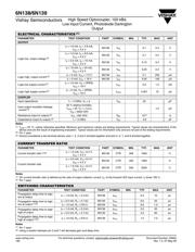
ELECTRICAL CHARACTERISTICS
(1)
PARAMETER TEST CONDITION PART SYMBOL MIN. TYP. MAX. UNIT
INPUT
Input forward voltage I
F
= 1.6 mA V
F
1.4 1.7 V
Input reverse breakdown voltage I
R
= 10 µA B
VR
5.0 V
Temperature coefficient of forward
voltage
I
F
= 1.6 mA - 1.8 mV/°C
器件 Datasheet 文档搜索
AiEMA 数据库涵盖高达 72,405,303 个元件的数据手册,每天更新 5,000 多个 PDF 文件
