Datasheet 搜索 > TI(德州仪器) > 74ACT11245 数据手册 > 74ACT11245 数据手册 3/24 页

¥ 0
74ACT11245 数据手册 - TI(德州仪器)
制造商:
TI(德州仪器)
描述:
具有三态输出的八路总线收发器
Pictures:
3D模型
符号图
焊盘图
引脚图
产品图
页面导航:
封装尺寸在P6P8P9P15P17P18
标记信息在P15P16
封装信息在P6P7P8P9P15P16P17P18
应用领域在P24

导航目录
74ACT11245数据手册
Page:
of 24 Go
若手册格式错乱,请下载阅览PDF原文件
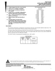
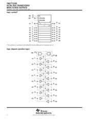
74ACT11245
OCTAL BUS TRANSCEIVER
WITH 3-STATE OUTPUTS
SCAS031C – JULY 1987 – REVISED APRIL 1996
3
POST OFFICE BOX 655303 • DALLAS, TEXAS 75265
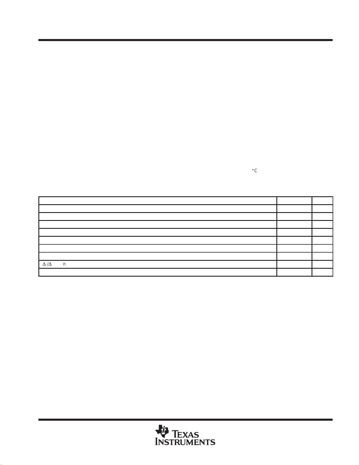
absolute maximum ratings over operating free-air temperature range (unless otherwise noted)
†
Supply voltage range, V
CC
–0.5 V to 7 V. . . . . . . . . . . . . . . . . . . . . . . . . . . . . . . . . . . . . . . . . . . . . . . . . . . . . . . . . .
Input voltage range, V
I
(see Note 1) –0.5 V to V
CC
+ 0.5 V. . . . . . . . . . . . . . . . . . . . . . . . . . . . . . . . . . . . . . . . . . .
Output voltage range, V
O
(see Note 1) –0.5 V to V
CC
+ 0.5 V. . . . . . . . . . . . . . . . . . . . . . . . . . . . . . . . . . . . . . . .
Input clamp current, I
IK
(V
I
< 0 or V
I
> V
CC
) ±20 mA. . . . . . . . . . . . . . . . . . . . . . . . . . . . . . . . . . . . . . . . . . . . . . . .
Output clamp current, I
OK
(V
O
< 0 or V
O
> V
CC
) ±50 mA. . . . . . . . . . . . . . . . . . . . . . . . . . . . . . . . . . . . . . . . . . . .
Continuous output current, I
O
(V
O
= 0 to V
CC
) ±50 mA. . . . . . . . . . . . . . . . . . . . . . . . . . . . . . . . . . . . . . . . . . . . . .
Continuous current through V
CC
or GND ±200 mA. . . . . . . . . . . . . . . . . . . . . . . . . . . . . . . . . . . . . . . . . . . . . . . . . .
Maximum power dissipation at T
A
= 55°C (in still air) (see Note 2):DB package 0.65 W. . . . . . . . . . . . . . . . . .
DW package 1.7 W. . . . . . . . . . . . . . . . . .
NT package 1.3 W. . . . . . . . . . . . . . . . . . .
PW package 0.7 W. . . . . . . . . . . . . . . . . . .
Storage temperature range, T
stg
–65°C to 150°C. . . . . . . . . . . . . . . . . . . . . . . . . . . . . . . . . . . . . . . . . . . . . . . . . . .
†
Stresses beyond those listed under “absolute maximum ratings” may cause permanent damage to the device. These are stress ratings only, and
functional operation of the device at these or any other conditions beyond those indicated under “recommended operating conditions” is not
implied. Exposure to absolute-maximum-rated conditions for extended periods may affect device reliability.
NOTES: 1. The input and output voltage ratings may be exceeded if the input and output current ratings are observed.
2. The maximum package power dissipation is calculated using a junction temperature of 150
_
C and a board trace length of 750 mils,
except for the NT package, which has a trace length of zero.
recommended operating conditions
MIN MAX UNIT
V
CC
Supply voltage 4.5 5.5 V
V
IH
High-level input voltage 2 V
V
IL
Low-level input voltage 0.8 V
V
I
Input voltage 0 V
CC
V
V
O
Output voltage 0 V
CC
V
I
OH
High-level output current –24 mA
I
OL
Low-level output current 24 mA
D
t/
D
v Input transition rise or fall rate 0 10 ns/V
T
A
Operating free-air temperature –40 85 °C
器件 Datasheet 文档搜索
AiEMA 数据库涵盖高达 72,405,303 个元件的数据手册,每天更新 5,000 多个 PDF 文件
