Datasheet 搜索 > 逻辑控制器 > Nexperia(安世) > 74HC00PW,118 数据手册 > 74HC00PW,118 数据手册 2/21 页

 器件3D模型
¥ 0.37
74HC00PW,118 数据手册 - Nexperia(安世)
制造商:
Nexperia(安世)
分类:
逻辑控制器
封装:
TSSOP-14
描述:
74HC00PW,118 编带
Pictures:
3D模型
符号图
焊盘图
引脚图
产品图
页面导航:
导航目录
74HC00PW,118数据手册
Page:
of 21 Go
若手册格式错乱,请下载阅览PDF原文件
SCLS181E − DECEMBER 1982 − REVISED AUGUST 2003
2
POST OFFICE BOX 655303 • DALLAS, TEXAS 75265
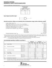
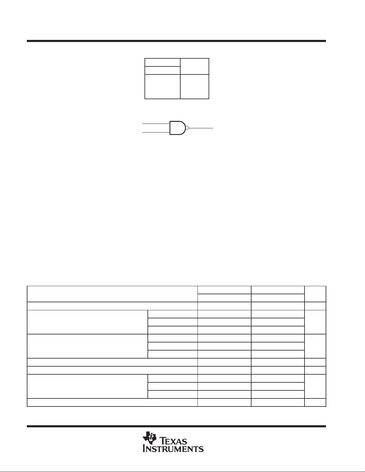
FUNCTION TABLE
(each gate)
INPUTS
OUTPUT
A B
OUTPUT
Y
H H L
L XH
X L H
logic diagram (positive logic)
A
B
Y
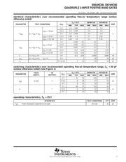
absolute maximum ratings over operating free-air temperature range (unless otherwise noted)
†
Supply voltage range, V
CC
−0.5 V to 7 V. . . . . . . . . . . . . . . . . . . . . . . . . . . . . . . . . . . . . . . . . . . . . . . . . . . . . . . . . .
Input clamp current, I
IK
(V
I
< 0 or V
I
> V
CC
) (see Note 1) ±20 mA. . . . . . . . . . . . . . . . . . . . . . . . . . . . . . . . . . . .
Output clamp current, I
OK
(V
O
< 0 or V
O
> V
CC
) (see Note 1) ±20 mA. . . . . . . . . . . . . . . . . . . . . . . . . . . . . . . .
Continuous output current, I
O
(V
O
= 0 to V
CC
) ±25 mA. . . . . . . . . . . . . . . . . . . . . . . . . . . . . . . . . . . . . . . . . . . . . .
Continuous current through V
CC
or GND ±50 mA. . . . . . . . . . . . . . . . . . . . . . . . . . . . . . . . . . . . . . . . . . . . . . . . . . .
Package thermal impedance, θ
JA
(see Note 2): D package 86°C/W. . . . . . . . . . . . . . . . . . . . . . . . . . . . . . . . . . .
DB package 96°C/W. . . . . . . . . . . . . . . . . . . . . . . . . . . . . . . . .
N package 80°C/W. . . . . . . . . . . . . . . . . . . . . . . . . . . . . . . . . . .
NS package 76°C/W. . . . . . . . . . . . . . . . . . . . . . . . . . . . . . . . .
PW package 113°C/W. . . . . . . . . . . . . . . . . . . . . . . . . . . . . . . .
Storage temperature range, T
stg
−65°C to 150°C. . . . . . . . . . . . . . . . . . . . . . . . . . . . . . . . . . . . . . . . . . . . . . . . . . .
†
Stresses beyond those listed under “absolute maximum ratings” may cause permanent damage to the device. These are stress ratings only, and
functional operation of the device at these or any other conditions beyond those indicated under “recommended operating conditions” is not
implied. Exposure to absolute-maximum-rated conditions for extended periods may affect device reliability.
NOTES: 1. The input and output voltage ratings may be exceeded if the input and output current ratings are observed.
2. The package thermal impedance is calculated in accordance with JESD 51-7.
recommended operating conditions (see Note 3)
SN54HC00 SN74HC00
UNIT
MIN NOM MAX MIN NOM MAX
UNIT
V
CC
Supply voltage 2 5 6 2 5 6 V
V
CC
= 2 V 1.5 1.5
V
IH
High-level input voltage
V
CC
= 4.5 V
3.15 3.15
V
V
IH
High-level input voltage
V
CC
= 6 V 4.2 4.2
V
V
CC
= 2 V 0.5 0.5
V
IL
Low-level input voltage
V
CC
= 4.5 V
1.35 1.35
V
V
IL
Low-level input voltage
V
CC
= 6 V 1.8 1.8
V
V
I
Input voltage 0 V
CC
0 V
CC
V
V
O
Output voltage 0 V
CC
0 V
CC
V
V
CC
= 2 V 1000 1000
∆t/∆v Input transition rise/fall time
V
CC
= 4.5 V
500 500
ns
∆t/∆v
Input transition rise/fall time
V
CC
= 6 V 400 400
ns
T
A
Operating free-air temperature −55 125 −40 85 °C
NOTE 3: All unused inputs of the device must be held at V
CC
or GND to ensure proper device operation. Refer to the TI application report,
Implications of Slow or Floating CMOS Inputs, literature number SCBA004.
器件 Datasheet 文档搜索
AiEMA 数据库涵盖高达 72,405,303 个元件的数据手册,每天更新 5,000 多个 PDF 文件
