Datasheet 搜索 > 逻辑控制器 > Nexperia(安世) > 74HC04PW,112 数据手册 > 74HC04PW,112 数据手册 4/16 页

 器件3D模型
¥ 1.932
74HC04PW,112 数据手册 - Nexperia(安世)
制造商:
Nexperia(安世)
分类:
逻辑控制器
封装:
TSSOP-14
描述:
Nexperia 74HC04PW,112 反相器, 电压输出, 2 → 6 V电源, 14引脚 TSSOP封装
Pictures:
3D模型
符号图
焊盘图
引脚图
产品图
页面导航:
导航目录
74HC04PW,112数据手册
Page:
of 16 Go
若手册格式错乱,请下载阅览PDF原文件
74HC_HCT04 All information provided in this document is subject to legal disclaimers. © NXP Semiconductors N.V. 2015. All rights reserved.
Product data sheet Rev. 5 — 27 November 2015 3 of 15
NXP Semiconductors
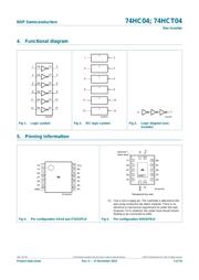
74HC04; 74HCT04
Hex inverter
5.1 Pin description
6. Functional description
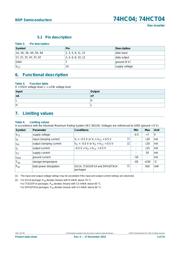
7. Limiting values
[1] The input and output voltage ratings may be exceeded if the input and output current ratings are observed.
[2] For SO14 package: P
tot
derates linearly with 8 mW/K above 70 C.
For (T)SSOP14 packages: P
tot
derates linearly with 5.5 mW/K above 60 C.
For DHVQFN14 packages: P
tot
derates linearly with 4.5 mW/K above 60 C.
Table 2. Pin description
Symbol Pin Description
1A, 2A, 3A, 4A, 5A, 6A 1, 3, 5, 9, 11, 13 data input
1Y, 2Y, 3Y, 4Y, 5Y, 6Y 2, 4, 6, 8, 10, 12 data output
GND 7 ground (0 V)
V
CC
14 supply voltage
Table 3. Function table
H = HIGH voltage level; L = LOW voltage level
Input Output
nA nY
LH
HL
Table 4. Limiting values
In accordance with the Absolute Maximum Rating System (IEC 60134). Voltages are referenced to GND (ground = 0 V).
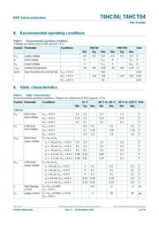
Symbol Parameter Conditions Min Max Unit
V
CC
supply voltage 0.5 +7 V
I
IK
input clamping current V
I
< 0.5 V or V
I
>V
CC
+0.5 V
[1]
- 20 mA
I
OK
output clamping current V
O
< 0.5 V or V
O
>V
CC
+0.5V
[1]
- 20 mA
I
O
output current 0.5 V < V
O
< V
CC
+0.5V - 25 mA
I
CC
supply current - 50 mA
I
GND
ground current 50 - mA
T
stg
storage temperature 65 +150 C
P
tot
total power dissipation SO14, (T)SSOP14 and DHVQFN14
packages
[2]
-500mW
器件 Datasheet 文档搜索
AiEMA 数据库涵盖高达 72,405,303 个元件的数据手册,每天更新 5,000 多个 PDF 文件
