Datasheet 搜索 > NXP(恩智浦) > 74HCT164 数据手册 > 74HCT164 数据手册 1/24 页

 器件3D模型
¥ 0.568
74HCT164 数据手册 - NXP(恩智浦)
制造商:
NXP(恩智浦)
封装:
SO-14
描述:
8位串行输入/并行输出移位寄存器 8-bit serial-in/parallel-out shift register
Pictures:
3D模型
符号图
焊盘图
引脚图
产品图
页面导航:
导航目录
74HCT164数据手册
Page:
of 24 Go
若手册格式错乱,请下载阅览PDF原文件
1. General description
The 74HC164; 74HCT164 are high-speed Si-gate CMOS devices and are pin compatible
with Low power Schottky TTL (LSTTL). They are specified in compliance with JEDEC
standard no. 7A.
The 74HC164; 74HCT164 are 8-bit edge-triggered shift registers with serial data entry
and an output from each of the eight stages. Data is entered serially through one of two
inputs (DSA or DSB); either input can be used as an active HIGH enable for data entry
through the other input. Both inputs must be connected together or an unused input must
be tied HIGH.
Data shifts one place to the right on each LOW-to-HIGH transition of the clock (CP) input
and enters into Q0, which is the logical AND of the two data inputs (DSA and DSB) that
existed one set-up time prior to the rising clock edge.
A LOW level on the master reset (MR) input overrides all other inputs and clears the
register asynchronously, forcing all outputs LOW.
2. Features
■ Gated serial data inputs
■ Asynchronous master reset
■ Complies with JEDEC standard no. 7A
■ ESD protection:
◆ HBM EIA/JESD22-A114-B exceeds 2000 V
◆ MM EIA/JESD22-A115-A exceeds 200 V.
■ Multiple package options
■ Specified from −40 °C to +85 °C and −40 °C to +125 °C.
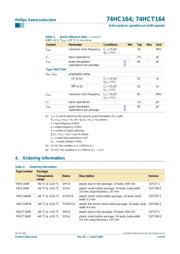
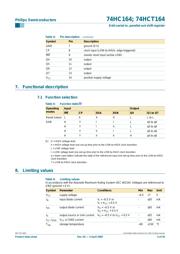
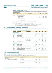
3. Quick reference data
74HC164; 74HCT164
8-bit serial-in, parallel-out shift register
Rev. 03 — 4 April 2005 Product data sheet
Table 1: Quick reference data
GND = 0 V; T
amb
= 25
°
C; t
r
= t
f
= 6 ns.
Symbol Parameter Conditions Min Typ Max Unit
Type 74HC164
t
PHL
, t
PLH
propagation delay
CP to Qn C
L
= 15 pF;
V
CC
= 5 V
-12-ns
MR to Qn C
L
= 15 pF;
V
CC
= 5 V
-11-ns
器件 Datasheet 文档搜索
AiEMA 数据库涵盖高达 72,405,303 个元件的数据手册,每天更新 5,000 多个 PDF 文件
