Datasheet 搜索 > 接口芯片 > Nexperia(安世) > 74LVC1G66GF,132 数据手册 > 74LVC1G66GF,132 数据手册 3/26 页

¥ 0.651
74LVC1G66GF,132 数据手册 - Nexperia(安世)
制造商:
Nexperia(安世)
分类:
接口芯片
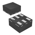
封装:
XFDFN-6
Pictures:
3D模型
符号图
焊盘图
引脚图
产品图
页面导航:
导航目录
74LVC1G66GF,132数据手册
Page:
of 26 Go
若手册格式错乱,请下载阅览PDF原文件

74LVC1G66 All information provided in this document is subject to legal disclaimers. © NXP Semiconductors N.V. 2016. All rights reserved.
Product data sheet Rev. 10 — 7 December 2016 2 of 25
NXP Semiconductors
74LVC1G66
Bilateral switch
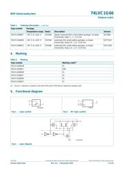
4. Marking
[1] The pin 1 indicator is located on the lower left corner of the device, below the marking code.
5. Functional diagram
74LVC1G66GF 40 C to +125 C XSON6 plastic extremely thin small outline package; no leads;
6 terminals; body 1 1 0.5 mm
SOT891
74LVC1G66GN 40 C to +125 C XSON6 extremely thin small outline package; no leads;
6 terminals; body 0.9 1.0 0.35 mm
SOT1115
74LVC1G66GS 40 C to +125 C XSON6 extremely thin small outline package; no leads;
6 terminals; body 1.0 1.0 0.35 mm
SOT1202
Table 1. Ordering information …continued
Type number Package
Temperature range Name Description Version
Table 2. Marking
Type number Marking code
[1]
74LVC1G66GW VL
74LVC1G66GV V66
74LVC1G66GM VL
74LVC1G66GF VL
74LVC1G66GN VL
74LVC1G66GS VL
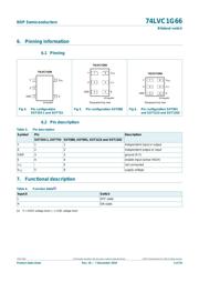
Fig 1. Logic symbol Fig 2. IEC logic symbol
DDJ
(
=<
PQD
;
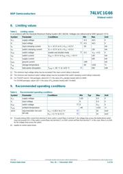
Fig 3. Logic diagram
DDP
9
&&
(
<
=
器件 Datasheet 文档搜索
AiEMA 数据库涵盖高达 72,405,303 个元件的数据手册,每天更新 5,000 多个 PDF 文件
