Datasheet 搜索 > 逻辑控制器 > NXP(恩智浦) > 74LVC2G17GN,132 数据手册 > 74LVC2G17GN,132 数据手册 8/19 页

¥ 1.157
74LVC2G17GN,132 数据手册 - NXP(恩智浦)
制造商:
NXP(恩智浦)
分类:
逻辑控制器
封装:
XFDFN-6
Pictures:
3D模型
符号图
焊盘图
引脚图
产品图
页面导航:
导航目录
74LVC2G17GN,132数据手册
Page:
of 19 Go
若手册格式错乱,请下载阅览PDF原文件
74LVC2G17 All information provided in this document is subject to legal disclaimers. © NXP B.V. 2013. All rights reserved.
Product data sheet Rev. 8 — 2 May 2013 8 of 19
NXP Semiconductors
74LVC2G17
Dual non-inverting Schmitt trigger with 5 V tolerant input
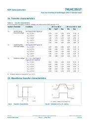
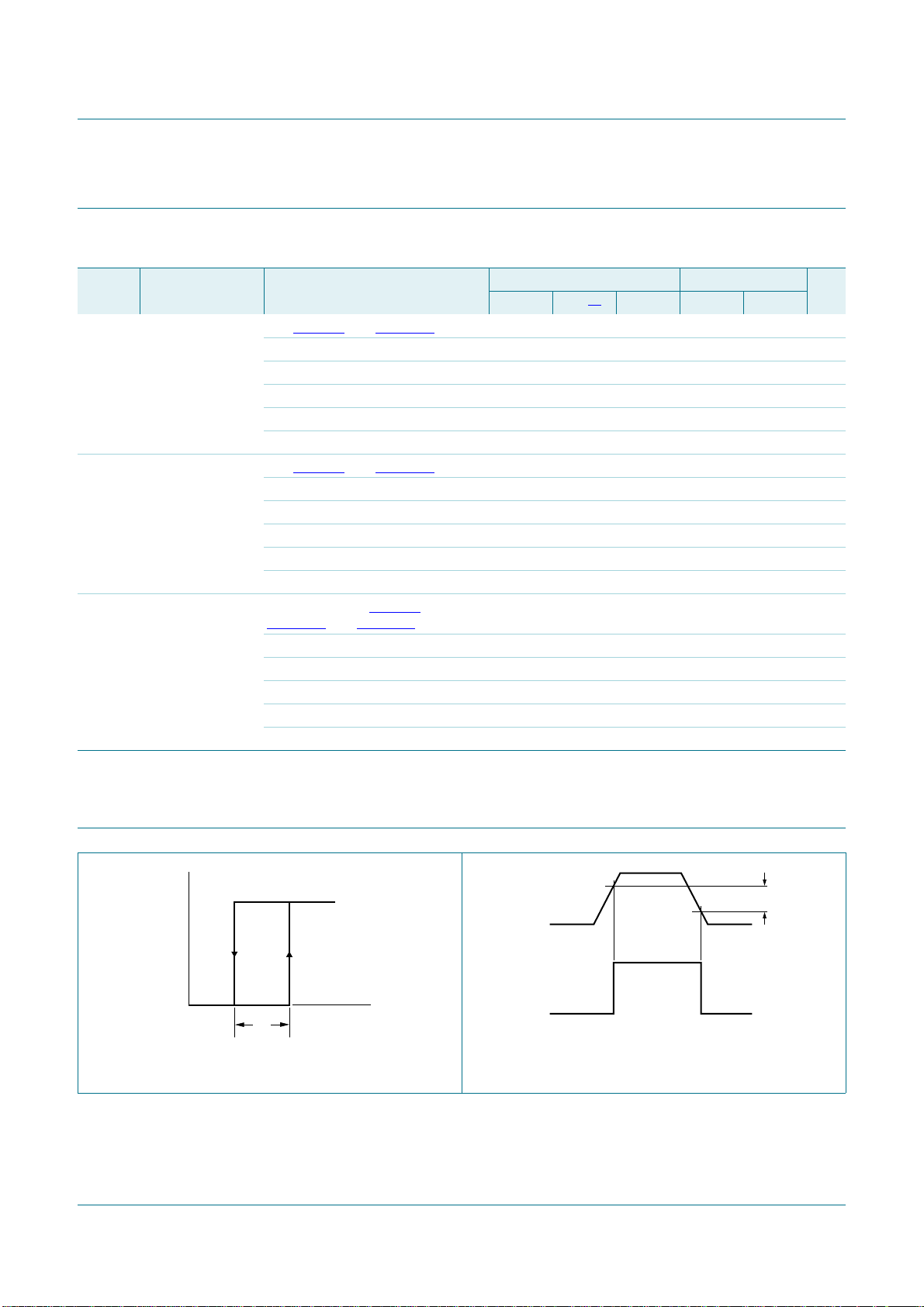
14. Transfer characteristics
[1] All typical values are measured at T
amb
=25C.
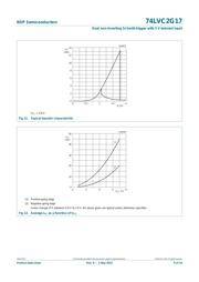
15. Waveforms transfer characteristics
Table 11. Transfer characteristics
At recommended operating conditions. Voltages are referenced to GND (ground = 0 V).
Symbol Parameter Conditions 40 C to +85 C 40 C to +125 C Unit
Min Typ
[1]
Max Min Max
V
T+
positive-going
threshold voltage
see Figure 9 and Figure 10
V
CC
= 1.8 V 0.70 1.10 1.50 0.70 1.70 V
V
CC
= 2.3 V 1.00 1.40 1.80 1.00 2.00 V
V
CC
= 3.0 V 1.30 1.76 2.20 1.30 2.40 V
V
CC
= 4.5 V 1.90 2.47 3.10 1.90 3.30 V
V
CC
= 5.5 V 2.20 2.91 3.60 2.20 3.80 V
V
T
negative-going
threshold voltage
see Figure 9 and Figure 10
V
CC
= 1.8 V 0.25 0.61 0.90 0.25 1.10 V
V
CC
= 2.3 V 0.40 0.80 1.15 0.40 1.35 V
V
CC
= 3.0 V 0.60 1.04 1.50 0.60 1.70 V
V
CC
= 4.5 V 1.00 1.55 2.00 1.00 2.20 V
V
CC
= 5.5 V 1.20 1.86 2.30 1.20 2.50 V
V
H
hysteresis voltage (V
T+
V
T
); see Figure 9,
Figure 10
and Figure 11
V
CC
= 1.8 V 0.15 0.49 1.00 0.15 1.20 V
V
CC
= 2.3 V 0.25 0.60 1.10 0.25 1.30 V
V
CC
= 3.0 V 0.40 0.73 1.20 0.40 1.40 V
V
CC
= 4.5 V 0.60 0.92 1.50 0.60 1.70 V
V
CC
= 5.5 V 0.70 1.02 1.70 0.70 1.90 V
V
T+
and V
T
limits at 70 % and 20 %.
Fig 9. Transfer characteristic Fig 10. Definition of V
T+
, V
T
and V
H
mnb154
V
O
V
H
V
I
V
T+
V
T−
mnb155
V
O
V
I
V
H
V
T+
V
T−
器件 Datasheet 文档搜索
AiEMA 数据库涵盖高达 72,405,303 个元件的数据手册,每天更新 5,000 多个 PDF 文件
