Datasheet 搜索 > 触发器 > NXP(恩智浦) > 74LVC2G74GT,115 数据手册 > 74LVC2G74GT,115 数据手册 1/25 页

¥ 0.724
74LVC2G74GT,115 数据手册 - NXP(恩智浦)
制造商:
NXP(恩智浦)
分类:
触发器
封装:
XFDFN-8
描述:
74LVC 系列 5.5 V 上升沿触发 D型触发器 表面贴装 -XSON-8
Pictures:
3D模型
符号图
焊盘图
引脚图
产品图
页面导航:
导航目录
74LVC2G74GT,115数据手册
Page:
of 25 Go
若手册格式错乱,请下载阅览PDF原文件

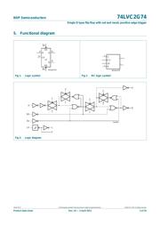
1. General description
The 74LVC2G74 is a single positive-edge triggered D-type flip-flop with individual data (D)
inputs, clock (CP) inputs, set (S
D) and reset (RD) inputs, and complementary Q and Q
outputs.
This device is fully specified for partial power-down applications using I
OFF
. The I
OFF
circuitry disables the output, preventing damaging backflow current through the device
when it is powered down.
The set and reset are asynchronous active LOW inputs and operate independently of the
clock input. Information on the data input is transferred to the Q output on the
LOW-to-HIGH transition of the clock pulse. The D inputs must be stable, one set-up time
prior to the LOW-to-HIGH clock transition for predictable operation.
Schmitt-trigger action at all inputs makes the circuit highly tolerant of slower input rise and
fall times.
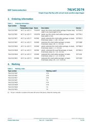
2. Features and benefits
Wide supply voltage range from 1.65 V to 5.5 V
5 V tolerant inputs for interfacing with 5 V logic
High noise immunity
Complies with JEDEC standard:
JESD8-7 (1.65 V to 1.95 V)
JESD8-5 (2.3 V to 2.7 V)
JESD8-B/JESD36 (2.7 V to 3.6 V)
24 mA output drive (V
CC
=3.0V)
ESD protection:
HBM JESD22-A114F exceeds 2000 V
MM JESD22-A115-A exceeds 200 V
CMOS low power consumption
Latch-up performance exceeds 250 mA
Direct interface with TTL levels
Inputs accept voltages up to 5 V
Multiple package options
Specified from 40 Cto+85C and 40 Cto+125C
74LVC2G74
Single D-type flip-flop with set and reset; positive edge trigger
Rev. 10 — 2 April 2013 Product data sheet
器件 Datasheet 文档搜索
AiEMA 数据库涵盖高达 72,405,303 个元件的数据手册,每天更新 5,000 多个 PDF 文件
