Datasheet 搜索 > 逻辑控制器 > Nexperia(安世) > 74LVC2T45DC-Q100H 数据手册 > 74LVC2T45DC-Q100H 数据手册 1/26 页
 器件3D模型
¥ 2.279
74LVC2T45DC-Q100H 数据手册 - Nexperia(安世)
制造商:
Nexperia(安世)
分类:
逻辑控制器
封装:
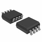
VSSOP-8
描述:
总线收发器 74LVC2T45DC-Q100/VSSOP8/REEL 7
Pictures:
3D模型
符号图
焊盘图
引脚图
产品图
页面导航:
典型应用电路图在P2
封装尺寸在P17P19P20
型号编码规则在P1P2
标记信息在P1P17P18
封装信息在P1P17P18P19P20
功能描述在P15
技术参数、封装参数在P3
应用领域在P18P26
电气规格在P5

导航目录
74LVC2T45DC-Q100H数据手册
Page:
of 26 Go
若手册格式错乱,请下载阅览PDF原文件
www.ti.com
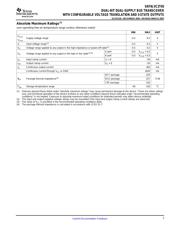
FEATURES
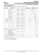
DCT OR DCU PACKAGE
(TOP VIEW)
1
2
3
4
8
7
6
5
V
CCA
A1
A2
GND
V
CCB
B1
B2
DIR
YZP PACKAGE
(BOTTOM VIEW)
A1
GND
B1
DIR
A2
B2
V
CCA
V
CCB
2
8
3
4
6
7
1
5
A1 A2
B2
C2
D2
B1
C1
D1
DESCRIPTION/ORDERING INFORMATION
SN74LVC2T45
DUAL-BIT DUAL-SUPPLY BUS TRANSCEIVER
WITH CONFIGURABLE VOLTAGE TRANSLATION AND 3-STATE OUTPUTS
SCES516I – DECEMBER 2003 – REVISED MARCH 2007
• Available in the Texas Instruments
NanoFree™ Package
• Fully Configurable Dual-Rail Design Allows
Each Port to Operate Over the Full 1.65-V to
5.5-V Power-Supply Range
• V
CC
Isolation Feature – If Either V
CC
Input Is at
GND, Both Ports Are in the High-Impedance
State
• DIR Input Circuit Referenced to V
CCA
• Low Power Consumption, 10- µ A Max I
CC
• ± 24-mA Output Drive at 3.3 V
• I
off
Supports Partial-Power-Down Mode
Operation
• Max Data Rates
– 420 Mbps (3.3-V to 5-V Translation)
– 210 Mbps (Translate to 3.3 V)
– 140 Mbps (Translate to 2.5 V)
– 75 Mbps (Translate to 1.8 V)
• Latch-Up Performance Exceeds 100 mA Per
JESD 78, Class II
• ESD Protection Exceeds JESD 22
– 4000-V Human-Body Model (A114-A)
– 200-V Machine Model (A115-A)
– 1000-V Charged-Device Model (C101)
This dual-bit noninverting bus transceiver uses two separate configurable power-supply rails. The A port is
designed to track V
CCA
. V
CCA
accepts any supply voltage from 1.65 V to 5.5 V. The B port is designed to track
V
CCB
. V
CCB
accepts any supply voltage from 1.65 V to 5.5 V. This allows for universal low-voltage bidirectional
translation between any of the 1.8-V, 2.5-V, 3.3-V, and 5-V voltage nodes.
ORDERING INFORMATION
T
A
PACKAGE
(1)
ORDERABLE PART NUMBER TOP-SIDE MARKING
(2)
NanoFree – WCSP (DSBGA)
Reel of 3000 SN74LVC2T45YZPR _ _ _TB_
0.23-mm Large Bump – YZP (Pb-free)
Reel of 3000 SN74LVC2T45DCTR
SSOP – DCT CT2_ _ _
–40 ° C to 85 ° C
Reel of 250 SN74LVC2T45DCTT
Reel of 3000 SN74LVC2T45DCUR
VSSOP – DCU CT2_
Reel of 250 SN74LVC2T45DCUT
(1) For the most current package and ordering information, see the Package Option Addendum at the end of this document, or see the TI
website at www.ti.com .
(2) DCT: The actual top-side marking has three additional characters that designate the year, month, and assembly/test site.
DCU: The actual top-side marking has one additional character that designates the assembly/test site.
YZP: The actual top-side marking has three preceding characters to denote year, month, and sequence code, and one following
character to designate the assembly/test site. Pin 1 identifier indicates solder-bump composition (1 = SnPb, • = Pb-free).
Please be aware that an important notice concerning availability, standard warranty, and use in critical applications of Texas
Instruments semiconductor products and disclaimers thereto appears at the end of this data sheet.
NanoFree is a trademark of Texas Instruments.
PRODUCTION DATA information is current as of publication date.
Copyright © 2003–2007, Texas Instruments Incorporated
Products conform to specifications per the terms of the Texas
Instruments standard warranty. Production processing does not
necessarily include testing of all parameters.
器件 Datasheet 文档搜索
AiEMA 数据库涵盖高达 72,405,303 个元件的数据手册,每天更新 5,000 多个 PDF 文件
