Datasheet 搜索 > SOC(赛元微) > A1010B-1PLG44I 数据手册 > A1010B-1PLG44I 数据手册 1/24 页
 器件3D模型
¥ 0
A1010B-1PLG44I 数据手册 - SOC(赛元微)
制造商:
SOC(赛元微)
封装:
LCC-44
Pictures:
3D模型
符号图
焊盘图
引脚图
产品图
页面导航:

导航目录
A1010B-1PLG44I数据手册
Page:
of 24 Go
若手册格式错乱,请下载阅览PDF原文件
April 1996
1-283
© 1996 Actel Corporation
ACT
™
1 Series FPGAs
Features
• 5V and 3.3V Families fully compatible with JEDEC
specifications
• Up to 2000 Gate Array Gates (6000 PLD equivalent gates)
• Replaces up to 50 TTL Packages
• Replaces up to twenty 20-Pin PAL
®
Packages
• Design Library with over 250 Macro Functions
• Gate Array Architecture Allows Completely Automatic
Place and Route
• Up to 547 Programmable Logic Modules
• Up to 273 Flip-Flops
• Data Rates to 75 MHz
• Two In-Circuit Diagnostic Probe Pins Support Speed
Analysis to 25 MHz
• Built-In High Speed Clock Distribution Network
• I/O Drive to 10 mA (5 V), 6 mA (3.3 V)
• Nonvolatile, User Programmable
• Fabricated in 1.0 micron CMOS technology
Description
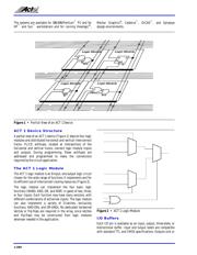
The ACT™ 1 Series of field programmable gate arrays
(FPGAs) offers a variety of package, speed, and application
combinations. Devices are implemented in silicon gate,
1-micron two-level metal CMOS, and they employ Actel’s
PLICE
®
antifuse technology. The unique architecture offers
gate array flexibility, high performance, and instant
turnaround through user programming. Device utilization is
typically 95 to 100 percent of available logic modules.
ACT 1 devices also provide system designers with unique
on-chip diagnostic probe capabilities, allowing convenient
testing and debugging. Additional features include an on-chip
clock driver with a hardwired distribution network. The
network provides efficient clock distribution with minimum
skew.
The user-definable I/Os are capable of driving at both TTL
and CMOS drive levels. Available packages include plastic
and ceramic J-leaded chip carriers, ceramic and plastic quad
flatpacks, and ceramic pin grid array.
A security fuse may be programmed to disable all further
programming and to protect the design from being copied or
reverse engineered.
Product Family Profile
The Designer and Designer
Advantage™ Systems
The ACT 1 device family is supported by Actel’s Designer and
Designer Advantage Systems, allowing logic design
implementation with minimum effort. The systems offer
Microsoft
®
Windows
™
and X Windows
™
graphical user
interfaces and integrate with the resident CAE system to
provide a complete gate array design environment: schematic
capture, simulation, fully automatic place and route, timing
verification, and device programming. The systems also
include the ACTmap
™
VHDL optimization and synthesis tool
and the ACTgen
™
Macro Builder, a powerful macro function
generator for counters, adders, and other structural blocks.
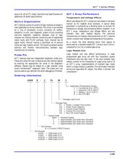
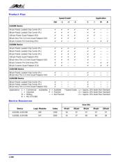
Device
A1010B
A10V10B
A1020B
A10V20B
Capacity
Gate Array Equivalent Gates
PLD Equivalent Gates
TTL Equivalent Packages
20-Pin PAL Equivalent Packages
1,200
3,000
30
12
2,000
6,000
50
20
Logic Modules 295 547
Flip-Flops (maximum) 147 273
Routing Resources
Horizontal Tracks/Channel
Vertical Tracks/Column
PLICE Antifuse Elements
22
13
112,000
22
13
186,000
User I/Os (maximum) 57 69
Packages: 44 PLCC
68 PLCC
100 PQFP
80 VQFP
84 CPGA
44 PLCC
68 PLCC
84 PLCC
100 PQFP
80 VQFP
84 CPGA
84 CQFP
Performance
5 V Data Rate (maximum)
3.3 V Data Rate (maximum)
75 MHz
55 MHz
75 MHz
55 MHz
Note:
See Product Plan on page 1-286 for package availability.
器件 Datasheet 文档搜索
AiEMA 数据库涵盖高达 72,405,303 个元件的数据手册,每天更新 5,000 多个 PDF 文件
