Datasheet 搜索 > SOC(赛元微) > A3PE3000-1FG484I 数据手册 > A3PE3000-1FG484I 数据手册 1/160 页
 器件3D模型
¥ 2597.402
A3PE3000-1FG484I 数据手册 - SOC(赛元微)
制造商:
SOC(赛元微)
封装:
BGA-484
Pictures:
3D模型
符号图
焊盘图
引脚图
产品图
页面导航:
引脚图在P95P96P98P99P100P102P104P106P108P110P112P114Hot
典型应用电路图在P61P64
型号编码规则在P2P3P148P150
封装信息在P3P95P96P98P149P151P152P153P155P157
功能描述在P6P148P153
技术参数、封装参数在P13P65P72P76P78P82P149
应用领域在P156P159
电气规格在P82
型号编号列表在P153

导航目录
A3PE3000-1FG484I数据手册
Page:
of 160 Go
若手册格式错乱,请下载阅览PDF原文件
June 2015 I
© 2015 Microsemi Corporation
ProASIC3E Flash Family FPGAs
with Optional Soft ARM Support
DS0098
Features and Benefits
High Capacity
• 600 k to 3 Million System Gates
• 108 to 504 kbits of True Dual-Port SRAM
• Up to 620 User I/Os
Reprogrammable Flash Technology
• 130-nm, 7-Layer Metal (6 Copper), Flash-Based CMOS
Process
• Instant On Level 0 Support
• Single-Chip Solution
• Retains Programmed Design when Powered Off
On-Chip User Nonvolatile Memory
• 1 kbit of FlashROM with Synchronous Interfacing
High Performance
• 350 MHz System Performance
• 3.3 V, 66 MHz 64-Bit PCI
In-System Programming (ISP) and Security
• ISP Using On-Chip 128-Bit Advanced Encryption Standard
(AES) Decryption via JTAG (IEEE 1532–compliant)
• FlashLock
®
Designed to Secure FPGA Contents
Low Power
• Core Voltage for Low Power
• Support for 1.5-V-Only Systems
• Low-Impedance Flash Switches
High-Performance Routing Hierarchy
• Segmented, Hierarchical Routing and Clock Structure
• Ultra-Fast Local and Long-Line Network
• Enhanced High-Speed, Very-Long-Line Network
• High-Performance, Low-Skew Global Network
• Architecture Supports Ultra-High Utilization
Pro (Professional) I/O
• 700 Mbps DDR, LVDS-Capable I/Os
• 1.5 V, 1.8 V, 2.5 V, and 3.3 V Mixed-Voltage Operation
• Bank-Selectable I/O Voltages—up to 8 Banks per Chip
• Single-Ended I/O Standards: LVTTL, LVCMOS 3.3 V /
2.5 V / 1.8 V / 1.5 V, 3.3 V PCI / 3.3 V PCI-X, and LVCMOS
2.5 V / 5.0 V Input
• Differential I/O Standards: LVPECL, LVDS, B-LVDS, and
M-LVDS
• Voltage-Referenced I/O Standards: GTL+ 2.5 V / 3.3 V, GTL
2.5 V / 3.3 V, HSTL Class I and II, SSTL2 Class I and II, SSTL3
Class I and II
• I/O Registers on Input, Output, and Enable Paths
• Hot-Swappable and Cold Sparing I/Os
• Programmable Output Slew Rate and Drive Strength
• Programmable Input Delay
• Schmitt Trigger Option on Single-Ended Inputs
• Weak Pull-Up/-Down
• IEEE 1149.1 (JTAG) Boundary Scan Test
• Pin-Compatible Packages across the ProASIC
®
3E Family
Clock Conditioning Circuit (CCC) and PLL
• Six CCC Blocks, Each with an Integrated PLL
• Configurable Phase-Shift, Multiply/Divide, Delay Capabilities
and External Feedback
• Wide Input Frequency Range (1.5 MHz to 350 MHz)
SRAMs and FIFOs
• Variable-Aspect-Ratio 4,608-Bit RAM Blocks (×1, ×2, ×4, ×9,
and ×18 organizations available)
• True Dual-Port SRAM (except ×18)
• 24 SRAM and FIFO Configurations with Synchronous Operation
up to 350 MHz
ARM
®
Processor Support in ProASIC3E FPGAs
• M1 ProASIC3E Devices—Cortex-M1 Soft Processor Available
with or without Debug
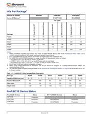
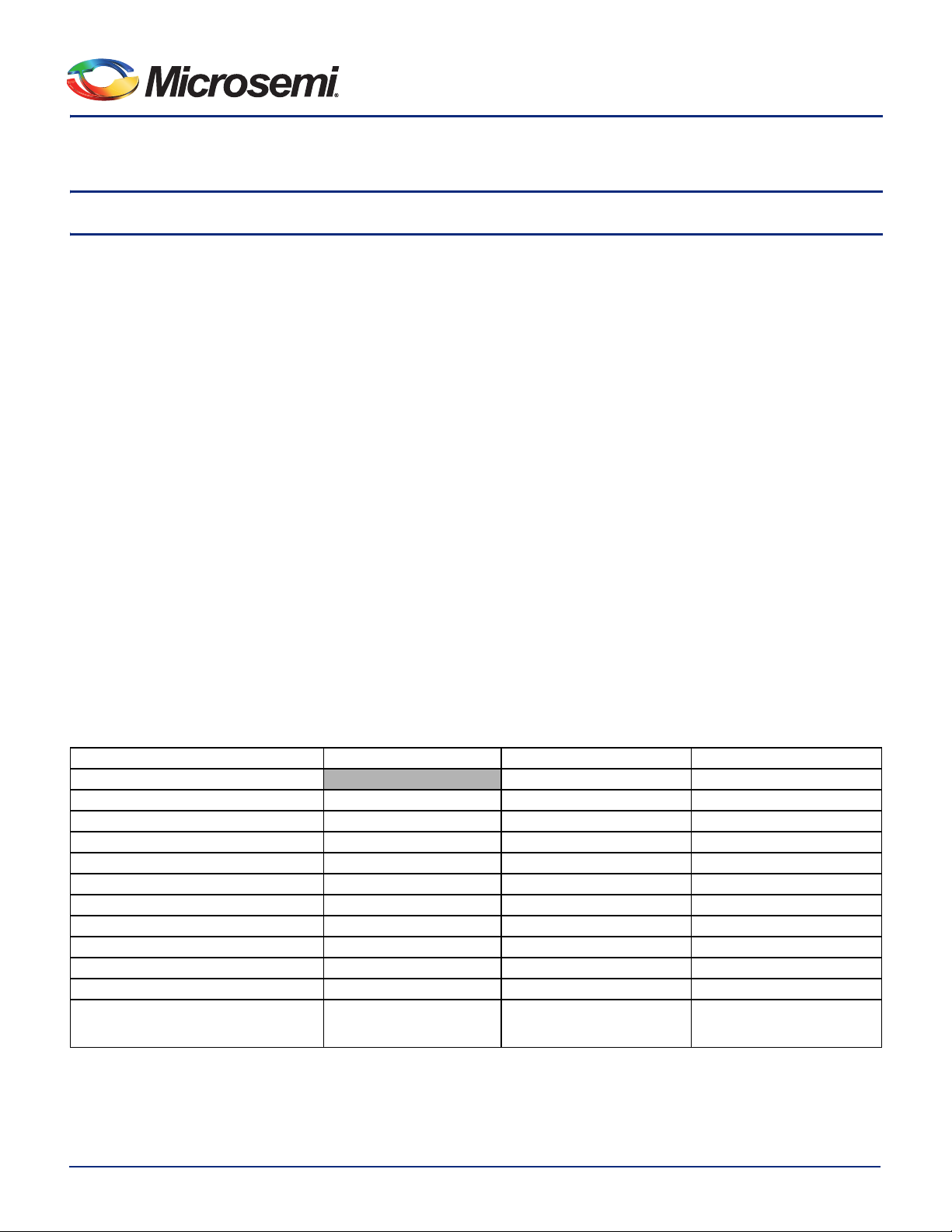
Table 1-1 • ProASIC3E Product Family
ProASIC3E Devices A3PE600 A3PE1500 A3PE3000
Cortex-M1 Devices
1
M1A3PE1500 M1A3PE3000
System Gates 600,000 1,500,000 3,000,000
VersaTiles (D-flip-flops) 13,824 38,400 75,264
RAM Kbits (1,024 bits) 108 270 504
4,608-Bit Blocks 24 60 112
FlashROM Kbits 11 1
Secure (AES) ISP Yes Yes Yes
CCCs with Integrated PLLs
2
66 6
VersaNet Globals
3
18 18 18
I/O Banks 88 8
Maximum User I/Os 270 444 620
Package Pins
PQFP
FBGA
PQ208
FG256, FG484
PQ208
FG484, FG676
PQ208
FG324
, FG484, FG896
Notes:
1. Refer to the Cortex-M1 product brief for more information.
2. The PQ208 package supports six CCCs and two PLLs.
3. Six chip (main) and three quadrant global networks are available.
4. For devices supporting lower densities, refer to the ProASIC3 Flash Family FPGAs datasheet.
Revision 15
器件 Datasheet 文档搜索
AiEMA 数据库涵盖高达 72,405,303 个元件的数据手册,每天更新 5,000 多个 PDF 文件
