Datasheet 搜索 > FPGA芯片 > Microsemi(美高森美) > A42MX16-3VQ100 数据手册 > A42MX16-3VQ100 数据手册 86/150 页
 器件3D模型
¥ 1029.484
A42MX16-3VQ100 数据手册 - Microsemi(美高森美)
制造商:
Microsemi(美高森美)
分类:
FPGA芯片
封装:
TQFP-100
Pictures:
3D模型
符号图
焊盘图
引脚图
产品图
页面导航:
引脚图在P18P20P88P90P91P92P94P96P98P100P102P104Hot
型号编码规则在P2P146
封装信息在P2P148
功能描述在P1P6P147
技术参数、封装参数在P22P23P24P25P26P27P28P29P146P148
电气规格在P23P25P27P146P148
导航目录
A42MX16-3VQ100数据手册
Page:
of 150 Go
若手册格式错乱,请下载阅览PDF原文件
40MX and 42MX FPGA Families
1-81 Revision 13
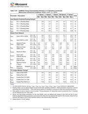
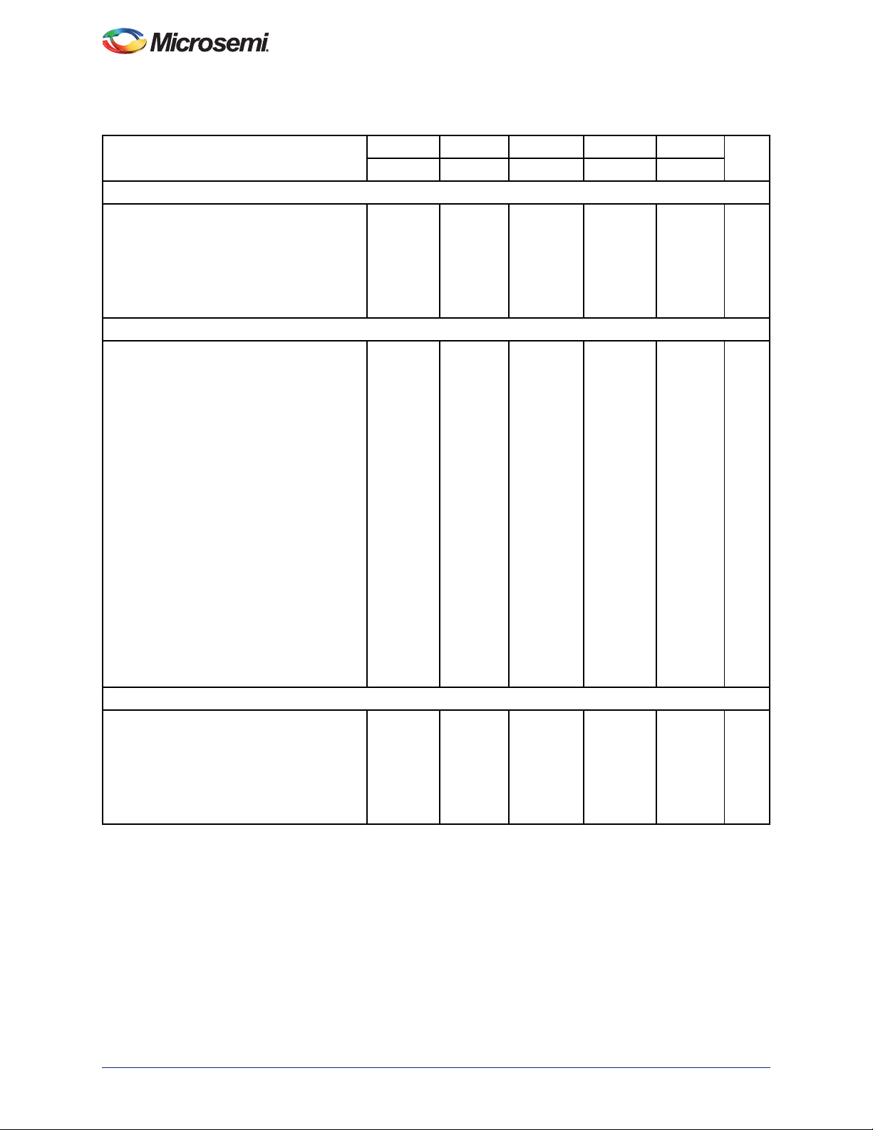
Input Module Predicted Routing Delays2
t
IRD1
FO = 1 Routing Delay 2.8 3.1 3.5 4.1 5.7 ns
t
IRD2
FO = 2 Routing Delay 3.2 3.5 4.1 4.8 6.7 ns
t
IRD3
FO = 3 Routing Delay 3.7 4.1 4.7 5.5 7.7 ns
t
IRD4
FO = 4 Routing Delay 4.2 4.6 5.3 6.2 8.7 ns
t
IRD8
FO = 8 Routing Delay 6.1 6.8 7.7 9.0 12.6 ns
Global Clock Network
t
CKH
Input LOW to HIGH
FO = 32
FO = 635
4.6
5.0
5.1
5.6
5.7
6.3
6.7
7.4
9.3
10.3
ns
ns
t
CKL
Input HIGH to LOW
FO = 32
FO = 635
5.3
6.8
5.9
7.6
6.7
8.6
7.8
10.1
11.0
14.1
ns
ns
t
PWH
Minimum Pulse
Width HIGH
FO = 32
FO = 635
2.5
2.8
2.7
3.1
3.1
3.5
3.6
4.1
5.1
5.7
ns
ns
t
PWL
Minimum Pulse
Width LOW
FO = 32
FO = 635
2.5
2.8
2.7
3.1
3.1
3.5
3.6
4.1
5.1
5.7
ns
ns
t
CKSW
Maximum Skew
FO = 32
FO = 635
1.0
1.0
1.2
1.2
1.3
1.3
1.5
1.5
2.2
2.2
ns
ns
t
SUEXT
Input Latch
External Set-Up
FO = 32
FO = 635
0.0
0.0
0.0
0.0
0.0
0.0
0.0
0.0
0.0
0.0
ns
ns
t
HEXT
Input Latch
External Hold
FO = 32
FO = 635
4.0
4.6
4.4
5.2
5.0
5.9
5.9
6.9
8.2
9.6
ns
ns
t
P
Minimum Period
(1/f
MAX
)
FO = 32
FO = 635
9.2
9.9
10.2
11.0
11.1
12.0
12.7
13.8
21.2
23.0
ns
ns
f
MAX
Maximum Datapath
Frequency
FO = 32
FO = 635
108
100
98
91
90
83
79
73
47
44
MHz
MHz
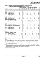
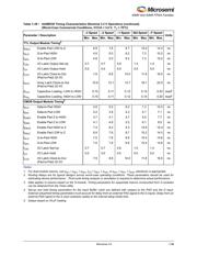
TTL Output Module Timing5
t
DLH
Data-to-Pad HIGH 3.6 4.0 4.5 5.3 7.4 ns
t
DHL
Data-to-Pad LOW 4.2 4.6 5.2 6.2 8.6 ns
t
ENZH
Enable Pad Z to HIGH 3.7 4.2 4.7 5.5 7.7 ns
t
ENZL
Enable Pad Z to LOW 4.1 4.6 5.2 6.1 8.5 ns
t
ENHZ
Enable Pad HIGH to Z 7.34 8.2 9.3 10.9 15.3 ns
Table 1-39 • A42MX36 Timing Characteristics (Nominal 3.3 V Operation) (continued)
(Worst-Case Commercial Conditions, VCCA = 3.0 V, T
J
= 70°C)
Parameter / Description
–3 Speed –2 Speed –1 Speed Std Speed –F Speed
Units
Min. Max. Min. Max. Min. Max. Min. Max. Min. Max.
Notes:
1. For dual-module macros, use t
PD1
+ t
RD1
+ t
PDn
, t
CO
+ t
RD1
+ t
PDn
, or t
PD1
+ t
RD1
+ t
SUD
, whichever is appropriate.
2. Routing delays are for typical designs across worst-case operating conditions. These parameters should be used for
estimating device performance. Post-route timing analysis or simulation is required to determine actual performance.
3. Data applies to macros based on the S-module. Timing parameters for sequential macros constructed from C-modules
can be obtained from the Timer utility.
4. Set-up and hold timing parameters for the Input Buffer Latch are defined with respect to the PAD and the D input.
External setup/hold timing parameters must account for delay from an external PAD signal to the G inputs. Delay from an
external PAD signal to the G input subtracts (adds) to the internal setup (hold) time.
5. Delays based on 35 pF loading.
器件 Datasheet 文档搜索
AiEMA 数据库涵盖高达 72,405,303 个元件的数据手册,每天更新 5,000 多个 PDF 文件
