Datasheet 搜索 > DA转换器 > ADI(亚德诺) > AD5062BRJZ-2500RL7 数据手册 > AD5062BRJZ-2500RL7 数据手册 5/20 页

¥ 7.239
AD5062BRJZ-2500RL7 数据手册 - ADI(亚德诺)
制造商:
ADI(亚德诺)
分类:
DA转换器
封装:
SOT-23-8
描述:
16 位,单通道,Analog Devices### 数字到模拟转换器 - Analog Devices
Pictures:
3D模型
符号图
焊盘图
引脚图
产品图
页面导航:
导航目录
AD5062BRJZ-2500RL7数据手册
Page:
of 20 Go
若手册格式错乱,请下载阅览PDF原文件
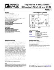
AD5062
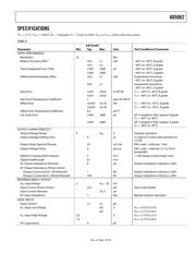
Rev. A | Page 5 of 20
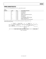
TIMING CHARACTERISTICS
V
DD
= 2.7 V to 5.5 V; all specifications T
MIN
to T
MAX
,
unless otherwise noted.
Table 3.
Parameter Limit
1
Unit Test Conditions/Comments
t
1
2
33 ns min SCLK cycle time
t
2
5 ns min SCLK high time
t
3
3 ns min SCLK low time
t
4
10 ns min
SYNC to SCLK falling edge setup time
t
5
3 ns min Data setup time
t
6
2 ns min Data hold time
t
7
0 ns min
SCLK falling edge to SYNC rising edge
t
8
12 ns min
Minimum SYNC high time
t
9
9 ns min
SYNC rising edge to next SCLK fall ignore
1
All input signals are specified with tr = tf = 1 ns/V (10% to 90% of V
DD
) and timed from a voltage level of (V
IL
+ V
IH
)/2.
2
Maximum SCLK frequency is 30 MHz.
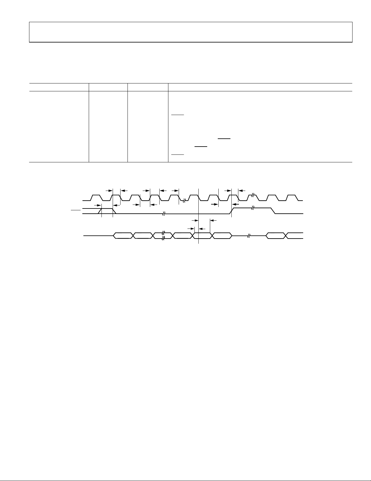
t
4
t
3
t
2
t
5
t
7
t
6
D0D1D2D22D23
SYNC
SCLK
04766-002
t
9
t
1
t
8
D23 D22DIN
Figure 2. Timing Diagram
器件 Datasheet 文档搜索
AiEMA 数据库涵盖高达 72,405,303 个元件的数据手册,每天更新 5,000 多个 PDF 文件
