Datasheet 搜索 > DA转换器 > ADI(亚德诺) > AD5062BRJZ-2500RL7 数据手册 > AD5062BRJZ-2500RL7 数据手册 7/20 页

¥ 7.239
AD5062BRJZ-2500RL7 数据手册 - ADI(亚德诺)
制造商:
ADI(亚德诺)
分类:
DA转换器
封装:
SOT-23-8
描述:
16 位,单通道,Analog Devices### 数字到模拟转换器 - Analog Devices
Pictures:
3D模型
符号图
焊盘图
引脚图
产品图
页面导航:
导航目录
AD5062BRJZ-2500RL7数据手册
Page:
of 20 Go
若手册格式错乱,请下载阅览PDF原文件
AD5062
Rev. A | Page 7 of 20
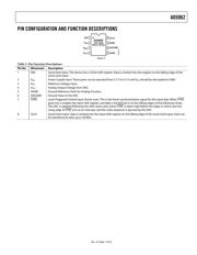
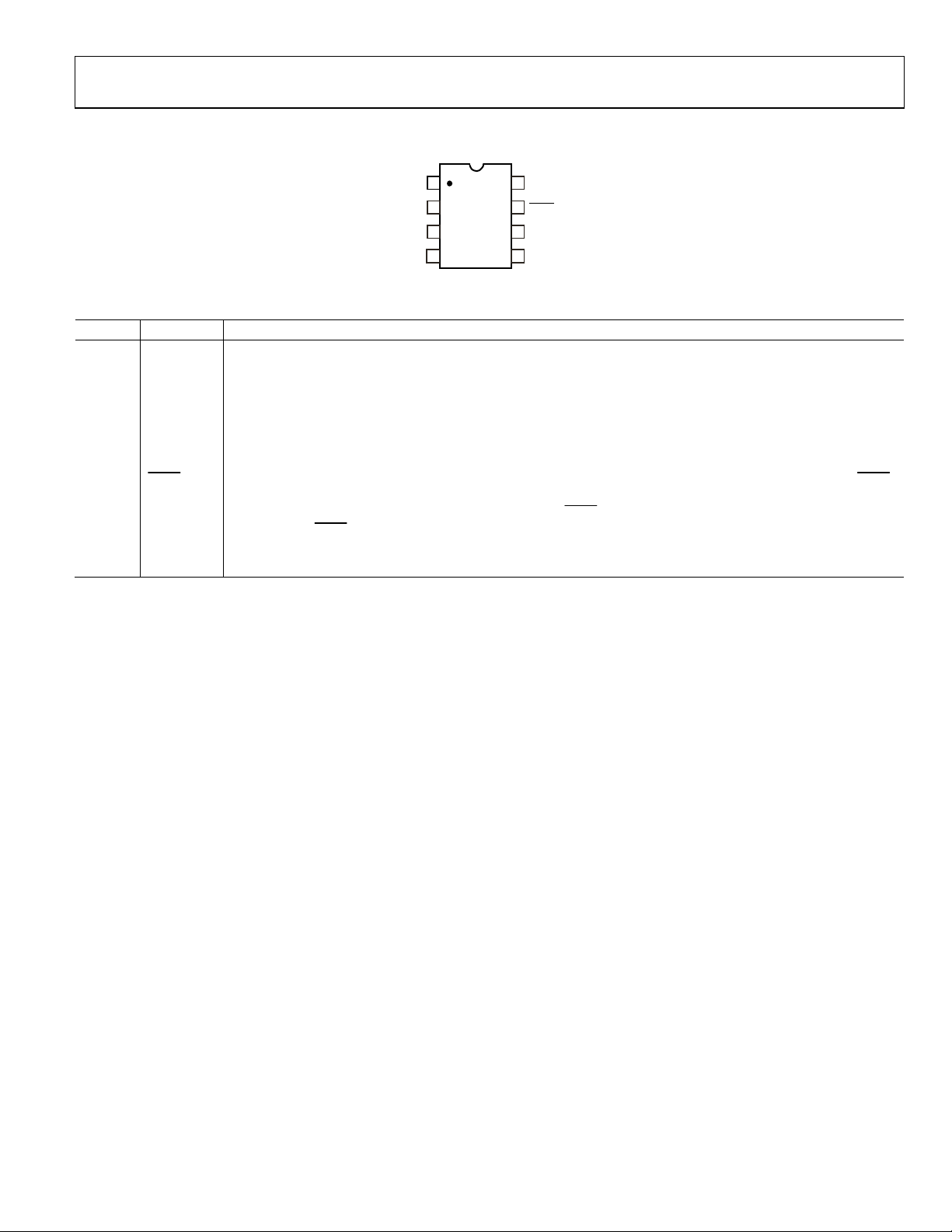
PIN CONFIGURATION AND FUNCTION DESCRIPTIONS
AD5062
TOP VIEW
(Not to Scale)
V
OUT
SYNC
18
AGND
SCLK
27
DIN
DACGND
36
04766-003
V
REF
45
V
DD
Figure 3.
Table 5. Pin Function Descriptions
Pin No. Mnemonic Description
1 DIN
Serial Data Input. This device has a 24-bit shift register. Data is clocked into the register on the falling edge of the
serial clock input.
2
V
DD
Power Supply Input. These parts can be operated from 2.7 V to 5.5 V, and V
DD
should be decoupled to GND.
3 V
REF
Reference Voltage Input.
4 V
OUT
Analog Output Voltage from DAC.
5 AGND Ground Reference Point for Analog Circuitry.
6 DACGND Ground Input to the DAC.
7
SYNC
Level-Triggered Control Input (Active Low). This is the frame synchronization signal for the input data. When SYNC
goes low, it enables the input shift register, and data is transferred in on the falling edges of the following clocks.
The DAC is updated following the 24th clock cycle unless SYNC
is taken high before this edge, in which case the
rising edge of SYNC acts as an interrupt, and the write sequence is ignored by the DAC.
8 SCLK
Serial Clock Input. Data is clocked into the input shift register on the falling edge of the serial clock input. Data can
be transferred at rates up to 30 MHz.
器件 Datasheet 文档搜索
AiEMA 数据库涵盖高达 72,405,303 个元件的数据手册,每天更新 5,000 多个 PDF 文件
