Datasheet 搜索 > DA转换器 > ADI(亚德诺) > AD5331BRU 数据手册 > AD5331BRU 数据手册 1/28 页

 器件3D模型
¥ 21.492
AD5331BRU 数据手册 - ADI(亚德诺)
制造商:
ADI(亚德诺)
分类:
DA转换器
封装:
TSSOP
描述:
2.5 V至5.5 V , 115微安,并行接口单电压输出8位/ 10位/ 12位DAC 2.5 V to 5.5 V, 115 uA, Parallel Interface Single Voltage-Output 8-/10-/12-Bit DACs
Pictures:
3D模型
符号图
焊盘图
引脚图
产品图
页面导航:
引脚图在P7P8P9P10P23Hot
典型应用电路图在P21
原理图在P1P7P8P9P10
封装尺寸在P24
型号编码规则在P25
焊接温度在P6
功能描述在P1P7P8P9P10
技术参数、封装参数在P1P3P6
应用领域在P1P21
电气规格在P13
导航目录
AD5331BRU数据手册
Page:
of 28 Go
若手册格式错乱,请下载阅览PDF原文件
2.5 V to 5.5 V, 115 μA, Parallel Interface
Single Voltage-Output 8-/10-/12-Bit DACs
AD5330/AD5331/AD5340/AD5341
Rev. A
Information furnished by Analog Devices is believed to be accurate and reliable. However, no
responsibility is assumed by Analog Devices for its use, nor for any infringements of patents or other
rights of third parties that may result from its use. Specifications subject to change without notice. No
license is granted by implication or otherwise under any patent or patent rights of Analog Devices.
Trademarks and registered trademarks are the property of their respective owners.
One Technology Way, P.O. Box 9106, Norwood, MA 02062-9106, U.S.A.
Tel: 781.329.4700 www.analog.com
Fax: 781.461.3113 ©2000–2008 Analog Devices, Inc. All rights reserved.
FEATURES
AD5330: single 8-bit DAC in 20-lead TSSOP
AD5331: single 10-bit DAC in 20-lead TSSOP
AD5340: single 12-bit DAC in 24-lead TSSOP
AD5341: single 12-bit DAC in 20-lead TSSOP
Low power operation: 115 μA @ 3 V, 140 μA @ 5 V
Power-down to 80 nA @ 3 V, 200 nA @ 5 V via
PD
Pin
2.5 V to 5.5 V power supply
Double-buffered input logic
Guaranteed monotonic by design over all codes
Buffered/unbuffered reference input options
Output range: 0 V to V
REF
or 0 V to 2 × V
REF
Power-on reset to 0 V
Simultaneous update of DAC outputs via
LDAC
pin
Asynchronous
CLR
facility
Low power parallel data interface
On-chip rail-to-rail output buffer amplifiers
Temperature range: −40°C to +105°C
APPLICATIONS
Portable battery-powered instruments
Digital gain and offset adjustment
Programmable voltage and current sources
Programmable attenuators
Industrial process control
GENERAL DESCRIPTION
The AD5330/AD5331/AD5340/AD5341
1
are single 8-/10-/12-
bit DACs. They operate from a 2.5 V to 5.5 V supply consuming
just 115 μA at 3 V and feature a power-down mode that further
reduces the current to 80 nA. The devices incorporate an on-chip
output buffer that can drive the output to both supply rails, but
the AD5330, AD5340, and AD5341 allow a choice of buffered
or unbuffered reference input.
The AD5330/AD5331/AD5340/AD5341 have a parallel
interface.
CS
selects the device and data is loaded into the
input registers on the rising edge of
WR
.
The GAIN pin allows the output range to be set at 0 V to V
REF
or
0 V to 2 × V
REF
.
Input data to the DACs is double-buffered, allowing simultane-
ous update of multiple DACs in a system using the
LDAC
pin.
An asynchronous
CLR
input is also provided, which resets the
contents of the input register and the DAC register to all zeros.
These devices also incorporate a power-on reset circuit that
ensures that the DAC output powers on to 0 V and remains
there until valid data is written to the device.
The AD5330/AD5331/AD5340/AD5341 are available in thin
shrink small outline packages (TSSOP).
1
Protected by U.S. Patent Number 5,969,657.
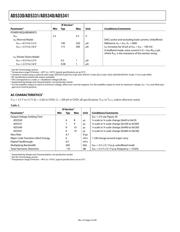
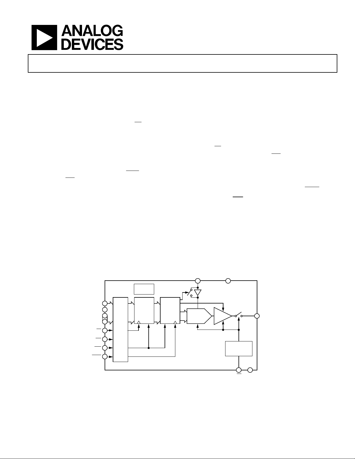
FUNCTIONAL BLOCK DIAGRAM
BUFFER
8-BIT
DAC
DAC
REGISTER
INPUT
REGISTER
INTERFACE LOGIC
POWER-DOWN
LOGIC
BUF
GAIN
DB
7
DB
0
.
.
CS
WR
CLR
LDAC
V
REF
V
DD
V
OUT
PD GND
AD5330
POWER-ON
RESET
RESET
10
9
7
6
13
20
8
1
3 12
4
11 5
0
6852-001
Figure 1. AD5330
器件 Datasheet 文档搜索
AiEMA 数据库涵盖高达 72,405,303 个元件的数据手册,每天更新 5,000 多个 PDF 文件
