Datasheet 搜索 > DA转换器 > ADI(亚德诺) > AD5360BSTZ-REEL 数据手册 > AD5360BSTZ-REEL 数据手册 10/28 页
 器件3D模型
¥ 430.523
AD5360BSTZ-REEL 数据手册 - ADI(亚德诺)
制造商:
ADI(亚德诺)
分类:
DA转换器
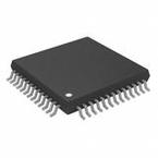
封装:
LQFP-52
Pictures:
3D模型
符号图
焊盘图
引脚图
产品图
页面导航:
引脚图在P10Hot
典型应用电路图在P20
原理图在P1
封装尺寸在P27
型号编码规则在P27
焊接温度在P9
功能描述在P3P10P15
技术参数、封装参数在P1P4P5P9
应用领域在P1
电气规格在P12
导航目录
AD5360BSTZ-REEL数据手册
Page:
of 28 Go
若手册格式错乱,请下载阅览PDF原文件
AD5360/AD5361
Rev. A | Page 10 of 28
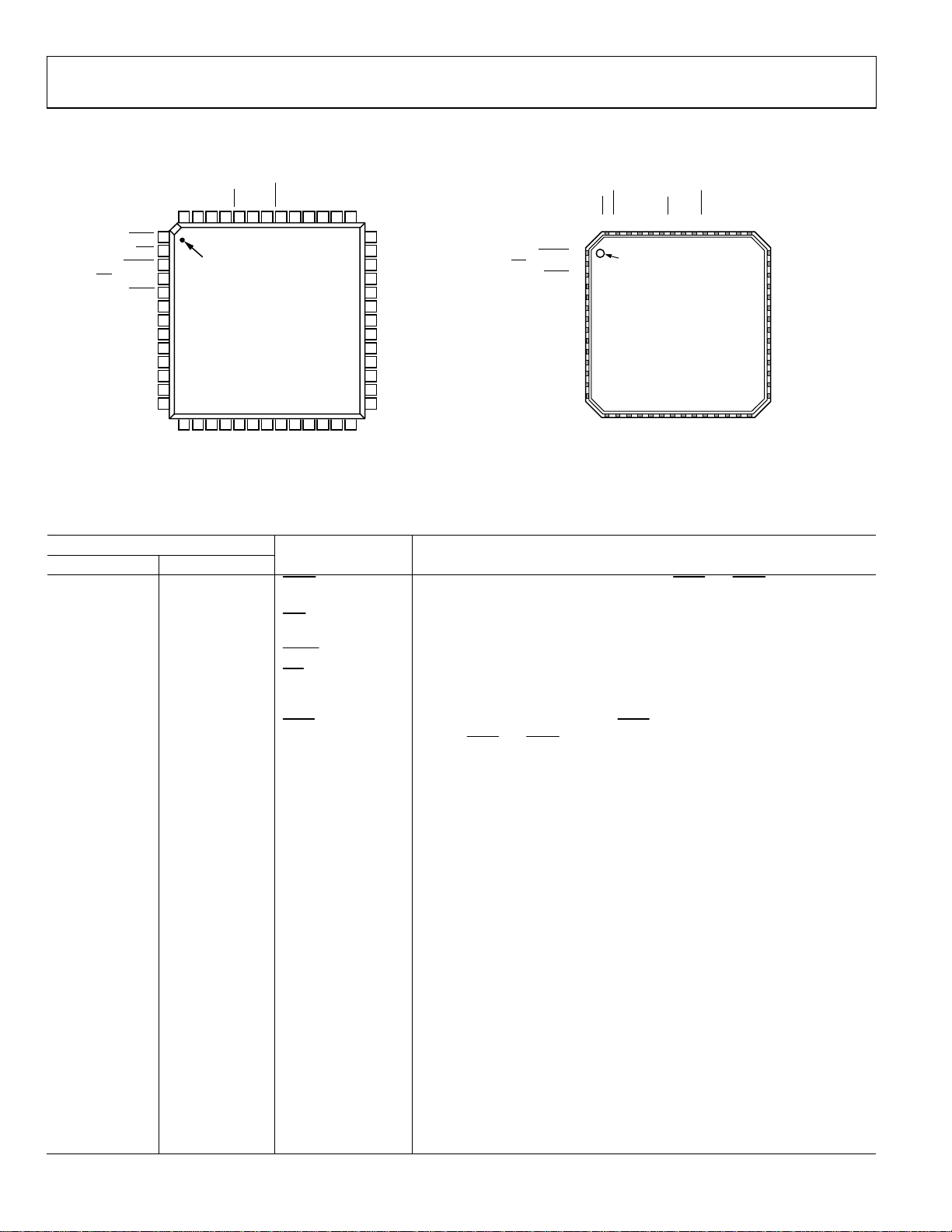
PIN CONFIGURATION AND FUNCTION DESCRIPTIONS
05761-022
52 51 50 49 48 43 42 41 4047 46 45 44
14 15 16 17 18 19 20 21 22 23 24 25 26
1
2
3
4
5
6
7
8
9
10
11
13
12
39
38
37
36
35
34
33
32
31
30
29
28
27
NC
VOUT8
VOUT9
VOUT10
VOUT11
SIGGND1
VOUT12
VOUT13
VOUT14
VOUT15
NC
NC
NC
LDAC
CLR
RESET
BIN/2SCOMP
BUSY
GPIO
MON_OUT
MON_IN0
NC
NC
V
DD
V
SS
VREF1
VOUT4
SIGGND0
VOUT3
VOUT2
VOUT1
VOUT0
TEMP_OUT
MON_IN1
VREF0
NC
V
SS
V
DD
NC
NC = NO CONNECT
AGND
DV
CC
SDO
PEC
SDI
SCLK
SYNC
DV
CC
DGND
VOUT
7
VOUT
6
VOUT
5
DGND
AD5360/
AD5361
PIN 1
INDICATOR
TOP VIEW
(Not to Scale)
PIN 1
INDICATOR
NC = NO CONNECT
1
RESET
2
BIN/2SCOMP
3
BUSY
4
GPIO
5
MON_OUT
6
MON_IN0
7
NC
8
NC
9
NC
10
NC
11
NC
12
V
DD
13
V
SS
14
VREF1
35
TEMP_OU
T
36
VOUT0
37
VOUT1
38
VOUT2
39
VOUT3
40
SIGGND0
41
VOUT4
42
VOUT5
34
MON_IN1
33
VREF0
32
NC
31
NC
30
V
SS
29
V
DD
15
NC
16
NC
17
VOUT8
19
VOUT10
21
SIGGND1
20
VOU
T11
22
VOUT12
23
V
OUT13
24
VOUT14
25
VOUT15
26
NC
27
NC
28
NC
18
VOUT9
45
DGND
46
DV
CC
47
SYNC
48
SCLK
49
SDI
50
PEC
51
SDO
52
DV
CC
53
D
GND
54
AGND
44
V
OUT7
43
VOUT6
TOP VIEW
(Not to Scale)
AD5360/
AD5361
55
LDAC
56
CLR
0
5761-028
Figure 7. 52-Lead LQFP Pin Configuration Figure 8. 56-Lead LFCSP Pin Configuration
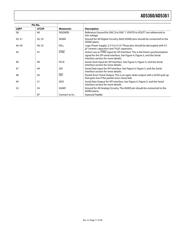
Table 5. LQFP Pin Function Descriptions
Pin No.
Mnemonic Description
LQFP LFCSP
1 55
LDAC
Load DAC Logic Input (Active Low). See the BUSY and LDAC Functions
section for more information.
2 56
CLR
Asynchronous Clear Input (Level Sensitive, Active Low). See the Clear
Function section for more information.
3 1
RESET
Digital Reset Input.
4 2
BIN
/2SCOMP Data Format Digital Input. Connecting this pin to DGND selects offset binary.
Connecting this pin to logic 1 selects twos complement. This input has a weak
pull-down.
5 3
BUSY
Digital Input/Open-Drain Output. BUSY is open drain when it is an output.
See the BUSY and LDAC Functions section for more information.
6 4 GPIO
Digital I/O Pin. This pin can be configured as an input or output that can be
read or programmed high or low via the serial interface. When configured as
an input, it has a weak pull-down.
7 5 MON_OUT
Analog Multiplexer Output. Any DAC output, the MON_IN0 input, or the
MON_IN1 input can be switched to this output.
8, 32 6, 34 MON_IN0, MON_IN1 Analog Multiplexer Inputs. Can be switched to MON_OUT.
9, 10, 14, 24, 25,
26, 27, 30
7 to 11, 15, 16,
26 to 28, 31, 32
NC No Connect.
11, 28 12, 29 V
DD
Positive Analog Power Supply; +9 V to +16.5 V for specified performance.
These pins should be decoupled with 0.1 μF ceramic capacitors and 10 μF
capacitors.
12, 29 13, 30 V
SS
Negative Analog Power Supply; −16.5 V to −8 V for specified performance.
These pins should be decoupled with 0.1 μF ceramic capacitors and 10 μF
capacitors.
13 14 VREF1 Reference Input for DAC 8 to DAC 15. This voltage is referred to AGND.
19 21 SIGGND1
Reference Ground for DAC 8 to DAC 15. VOUT8 to VOUT15 are referenced to
this voltage.
31 33 VREF0 Reference Input for DAC 0 to DAC 7. This voltage is referred to AGND.
33 35 TEMP_OUT
Provides an output voltage proportional to chip temperature. This is typically
1.46 V at 25°C with an output variation of 4.4 mV/°C.
34 to 37, 39 to
42, 15 to 18, 20
to 23
36 to 39, 41 to
44, 17 to 20, 22
to 25
VOUT0 to VOUT15
DAC Outputs. Buffered analog outputs for each of the 16 DAC channels. Each
analog output is capable of driving an output load of 10 kΩ to ground.
Typical output impedance of these amplifiers is 0.5 Ω.
器件 Datasheet 文档搜索
AiEMA 数据库涵盖高达 72,405,303 个元件的数据手册,每天更新 5,000 多个 PDF 文件
