Datasheet 搜索 > 运算放大器 > ADI(亚德诺) > AD549LH 数据手册 > AD549LH 数据手册 1/18 页

¥ 6.913
AD549LH 数据手册 - ADI(亚德诺)
制造商:
ADI(亚德诺)
分类:
运算放大器
封装:
TO-99-8
描述:
ANALOG DEVICES AD549LH 运算放大器, 单路, 1 MHz, 1个放大器, 3 V/µs, ± 5V 至 ± 18V, TO-99, 8 引脚
Pictures:
3D模型
符号图
焊盘图
引脚图
产品图
页面导航:
导航目录
AD549LH数据手册
Page:
of 18 Go
若手册格式错乱,请下载阅览PDF原文件
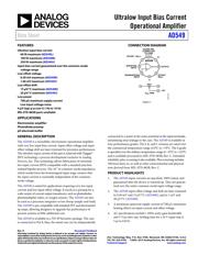
Ultralow Input Bias Current
Operational Amplifier
Data Sheet
AD549
Rev. K Document Feedback
Information furnished by Analog Devices is believed to be accurate and reliable. However, no
responsibility is assumed by Analog Devices for its use, nor for any infringements of patents or other
rights of third parties that may result from its use. Specifications subject to change without notice. No
license is granted by implication or otherwise under any patent or patent rights of Analog Devices.
Trademarks and registered trademarks are the property of their respective owners.
One Technology Way, P.O. Box 9106, Norwood, MA 02062-9106, U.S.A.
Tel: 781.329.4700 ©2002–2015 Analog Devices, Inc. All rights reserved.
Technical Support www.analog.com
FEATURES
Ultralow input bias current
60 fA maximum (AD549L)
100 fA maximum (AD549K)
250 fA maximum (AD549J)
Input bias current guaranteed over the common-mode
voltage range
Low offset voltage
0.50 mV maximum (AD549K)
1.00 mV maximum (AD549J)
Low offset drift
15 μV/°C maximum (AD549K)
20 μV/°C maximum (AD549J)
Low power
700 μA maximum supply current
Low input voltage noise
4 μV (typ) p-p over 0.1 Hz to 10 Hz
MIL-STD-883B parts available
APPLICATIONS
Electrometer amplifier
Photodiode preamp
pH electrode buffer
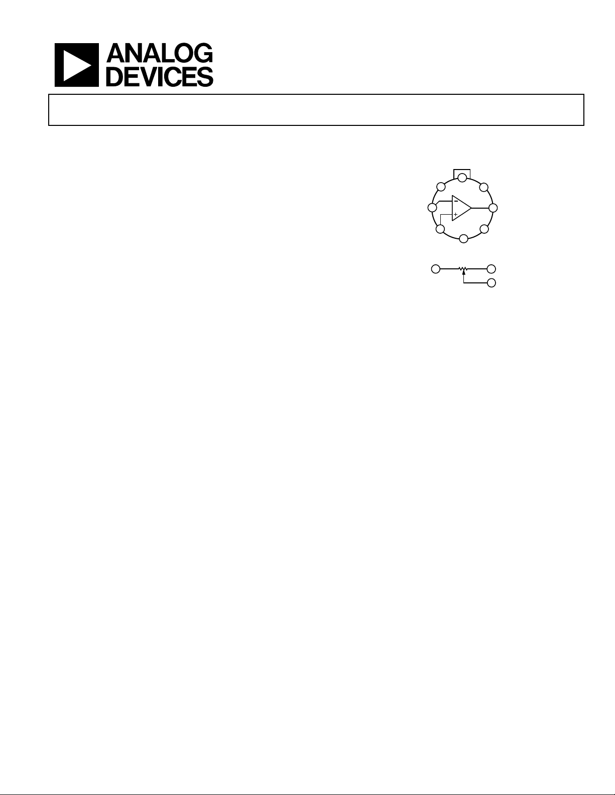
CONNECTION DIAGRAM
00511-001
AD549
OFFSET NULL
OUTPUT
V–
OFFSET
NULL
NONINVERTIN
G
INPUT
V+
GUARD PIN,
CONNECTED
TO CASE
INVERTING
INPUT
V
OS
TRIM
–15V
10kΩ
6
1
5
4
7
3
2
8
1
5
4
Figure 1.
GENERAL DESCRIPTION
The AD549 is a monolithic electrometer operational amplifier
with very low input bias current. Input offset voltage and input
offset voltage drift are laser trimmed for precision performance.
The ultralow input current of the part is achieved with Topgate™
JFET technology, a process development exclusive to Analog
Devices, Inc. This technology allows fabrication of extremely
low input current JFETs compatible with a standard junction
isolated bipolar process. The 10
15
Ω common-mode impedance,
which results from the bootstrapped input stage, ensures that
the input current is essentially independent of the common-
mode voltage.
The AD549 is suited for applications requiring very low input
current and low input offset voltage. It excels as a preamp for a
wide variety of current output transducers, such as photodiodes,
photomultiplier tubes, or oxygen sensors. The AD549 can also
be used as a precision integrator or low droop sample-and-hold.
The AD549 is pin compatible with standard FET and electrometer
op amps, allowing designers to upgrade the performance of
present systems at little additional cost.
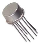
The AD549 is available in a TO-99 hermetic package. The case
is connected to Pin 8, thus, the metal case can be independently
connected to a point at the same potential as the input terminals,
minimizing stray leakage to the case. The AD549 is available in
four performance grades. The J, K, and L versions are rated over
the commercial temperature range of 0°C to +70°C. The S grade
is specified over the military temperature range of −55°C to +125°C
and is available processed to MIL-STD-883B, Rev. C. Extended
reliability plus screening is also available. Plus screening includes
168 hour burn-in, as well as other environmental and physical
tests derived from MIL-STD-883B, Rev. C.
PRODUCT HIGHLIGHTS
1. The AD549 input currents are specified, 100% tested, and
guaranteed after the device is warmed up. They are guaran-
teed over the entire common-mode input voltage range.
2. The AD549 input offset voltage and drift are laser trimmed
to 0.50 mV and 15 μV/°C (AD549K), and to 1 mV and
20 μV/°C (AD549J).
3. A maximum quiescent supply current of 700 μA minimizes
heating effects on input current and offset voltage.
4. AC specifications include 1 MHz unity-gain bandwidth
and 3 V/μs slew rate. Settling time for a 10 V input step is
5 μs to 0.01%.
器件 Datasheet 文档搜索
AiEMA 数据库涵盖高达 72,405,303 个元件的数据手册,每天更新 5,000 多个 PDF 文件
