Datasheet 搜索 > 运算放大器 > ADI(亚德诺) > AD648JR 数据手册 > AD648JR 数据手册 1/12 页
 器件3D模型
¥ 9.637
AD648JR 数据手册 - ADI(亚德诺)
制造商:
ADI(亚德诺)
分类:
运算放大器
封装:
SOIC
描述:
双路精密,低功耗BiFET运算放大器 Dual Precision, Low Power BiFET Op Amp
Pictures:
3D模型
符号图
焊盘图
引脚图
产品图
页面导航:
封装信息在P1P3
技术参数、封装参数在P2P3
电气规格在P5


导航目录
AD648JR数据手册
Page:
of 12 Go
若手册格式错乱,请下载阅览PDF原文件
REV. E
Information furnished by Analog Devices is believed to be accurate and
reliable. However, no responsibility is assumed by Analog Devices for its
use, nor for any infringements of patents or other rights of third parties that
may result from its use. No license is granted by implication or otherwise
under any patent or patent rights of Analog Devices.
a
Dual Precision,
Low Power BiFET Op Amp
AD648
FEATURES
DC Performance
400 A max Quiescent Current
10 pA max Bias Current, Warmed Up (AD648B)
1 V max Offset Voltage (AD648B)
10 V/ⴗC max Drift (AD648B)
2 V p-p Noise, 0.1 Hz to 10 Hz
AC Performance
1.8 V/ s Slew Rate
1 MHz Unity Gain Bandwidth
Available in Plastic Mini-DIP, CERDIP, and Plastic SOIC
Packages
MIL-STD-883B Parts Available
Surface Mount (SOIC) Package Available in Tape and
Reel in Accordance with EIA-481A Standard
Single Version: AD548
PRODUCT DESCRIPTION
The AD648 is a matched pair of low power, precision mono-
lithic operational amplifiers. It offers both low bias current
(10 pA max, warmed up) and low quiescent current (400 µA
max) and is fabricated with ion-implanted FET and laser wafer
trimming technologies. Input bias current is guaranteed over the
AD648’s entire common-mode voltage range.
The economical J grade has a maximum guaranteed offset
voltage of less than 2 mV and an offset voltage drift of less than
20 µV/°C. This level of dc precision is achieved using Analog’s
laser wafer drift trimming process. The combination of low
quiescent current and low offset voltage drift minimizes changes
in input offset voltage due to self-heating effects. Five grades are
offered over the commercial, industrial and military temperature
ranges.
The AD648 is recommended for any dual supply op amp
application requiring low power and excellent dc and ac per-
formance. In applications such as battery-powered, precision
instrument front ends and CMOS DAC buffers, the AD648’s
excellent combination of low input offset voltage and drift, low
bias current, and low 1/f noise reduces output errors. High
common-mode rejection (82 dB, min on the “B” grade) and
high open-loop gain ensures better than 12-bit linearity in high
impedance, buffer applications.
The AD648 is pinned out in a standard dual op amp configura-
tion and is available in seven performance grades. The AD648J
and AD648K are rated over the commercial temperature range
of 0°C to 70°C. The AD648 and AD648B are rated over the
industrial temperature range of –40°C to +85°C. The AD648S
and AD648T are rated over the military temperature range of
–55°C to +125°C and the AD648T* grade is available pro-
cessed to MIL-STD-883B, Rev. C.
The AD648 is available in an 8-lead plastic mini-DIP,
CERDIP, and SOIC.
*Not for new design, obsolete April 2002.
PRODUCT HIGHLIGHTS
1. A combination of low supply current, excellent dc and ac
performance and low drift makes the AD648 the ideal op
amp for high performance, low power applications.
2. The AD648 is pin compatible with industry standard dual
op amps such as the LF442, TL062, and AD642, enabling
designers to improve performance while achieving a reduc-
tion in power dissipation of up to 85%.
3. Guaranteed low input offset voltage (2 mV max) and drift
(20 µV/°C max) for the AD648J are achieved using Analog
Devices’ laser drift trimming technology.
4. Analog Devices specifies each device in the warmed-up
condition, insuring that the device will meet its published
specifications in actual use.
5. Matching characteristics are excellent for all grades. The
input offset voltage matching between amplifiers in the
AD648J is within 2 mV.
6. Crosstalk between amplifiers is less than –120 dB at 1 kHz.
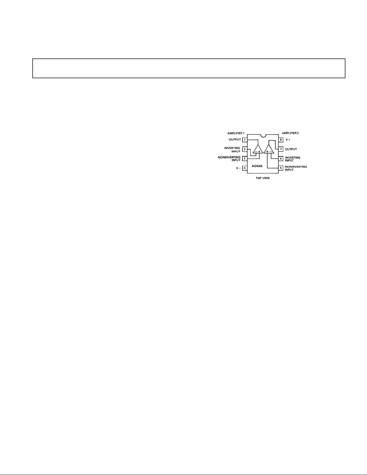
CONNECTION DIAGRAM
Plastic Mini-Dip (N) Package,
Plastic SOIC (R) Package
and
CERDIP (Q) Package
One Technology Way, P.O. Box 9106, Norwood, MA 02062-9106, U.S.A.
Tel: 781/329-4700www.analog.com
Fax: 781/326-8703 © Analog Devices, Inc., 2002
器件 Datasheet 文档搜索
AiEMA 数据库涵盖高达 72,405,303 个元件的数据手册,每天更新 5,000 多个 PDF 文件
