Datasheet 搜索 > DA转换器 > ADI(亚德诺) > AD7302BN 数据手册 > AD7302BN 数据手册 1/16 页
 器件3D模型
¥ 30.022
AD7302BN 数据手册 - ADI(亚德诺)
制造商:
ADI(亚德诺)
分类:
DA转换器
封装:
DIP-20
描述:
2.7 V至5.5 V ,并行输入双电压输出8位DAC 2.7 V to 5.5 V, Parallel Input Dual Voltage Output 8-Bit DAC
Pictures:
3D模型
符号图
焊盘图
引脚图
产品图
页面导航:
导航目录
AD7302BN数据手册
Page:
of 16 Go
若手册格式错乱,请下载阅览PDF原文件
REV. 0
Information furnished by Analog Devices is believed to be accurate and
reliable. However, no responsibility is assumed by Analog Devices for its
use, nor for any infringements of patents or other rights of third parties
which may result from its use. No license is granted by implication or
otherwise under any patent or patent rights of Analog Devices.
a
AD7302
One Technology Way, P.O. Box 9106, Norwood, MA 02062-9106, U.S.A.
Tel: 617/329-4700 World Wide Web Site: http://www.analog.com
Fax: 617/326-8703 © Analog Devices, Inc., 1997
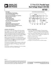
2.7 V to 5.5 V, Parallel Input
Dual Voltage Output 8-Bit DAC
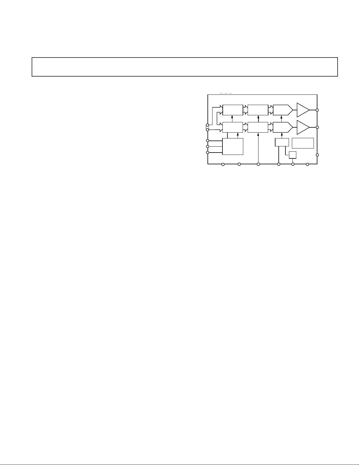
FUNCTIONAL BLOCK DIAGRAM
POWER ON
RESET
CS
WR
D0
REFIN
V
DD
AD7302
V
OUT
A
DGND
D7
AGND
A/B
CLR
LDAC
PD
I/V
V
OUT
B
MUX
÷2
INPUT
REGISTER
DAC
REGISTER
I DAC A
DAC
REGISTER
I DAC B
I/V
INPUT
REGISTER
CONTROL
LOGIC
FEATURES
Two 8-Bit DACs In One Package
20-Lead DIP/SOIC/TSSOP Package
+2.7 V to +5.5 V Operation
Internal and External Reference Capability
DAC Power-Down Function
Parallel Interface
On-Chip Output Buffer
Rail-to-Rail Operation
Low Power Operation 3 mA max @ 3.3 V
Power-Down to 1 mA max @ 258C
APPLICATIONS
Portable Battery Powered Instruments
Digital Gain and Offset Adjustment
Programmable Voltage and Current Sources
Programmable Attenuators
GENERAL DESCRIPTION
The AD7302 is a dual, 8-bit voltage out DAC that operates
from a single +2.7 V to +5.5 V supply. Its on-chip precision
output buffers allow the DAC outputs to swing rail to rail. The
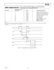
AD7302 has a parallel microprocessor and DSP-compatible
interface with high speed registers and double buffered interface
logic. Data is loaded to the registers on the rising edge of CS or
WR and the A/B pin selects either DAC A or DAC B.
Reference selection for AD7302 can be either an internal
reference derived from the V
DD
or an external reference applied
at the REFIN pin. Both DACs can be simultaneously updated
using the asynchronous LDAC input and can be cleared by
using the asynchronous CLR input.
The low power consumption of this part makes it ideally suited
to portable battery operated equipment. The power consump-
tion is less than 10 mW at 3.3 V, reducing to 3 µW in power-
down mode.
The AD7302 is available in a 20-pin plastic dual-in-line package,
20-lead SOIC and a 20-lead TSSOP package.
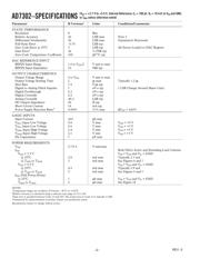
PRODUCT HIGHLIGHTS
1.␣ Low Power, Single Supply Operation. This part operates
from a single +2.7 V to +5.5 V supply and typically consumes
15 mW at 5 V, making it ideal for battery powered applications.
2.␣ The on-chip output buffer amplifiers allow the outputs of the
DACs to swing rail to rail with a settling time of typically 1.2 µs.
3.␣ Internal or external reference capability.
4.␣ High speed parallel interface.
5. Power-Down Capability. When powered down the DAC
consumes less than 1 µA at 25°C.
6. Packaged in 20-lead DIP, SOIC and TSSOP packages.
器件 Datasheet 文档搜索
AiEMA 数据库涵盖高达 72,405,303 个元件的数据手册,每天更新 5,000 多个 PDF 文件
