Datasheet 搜索 > AD转换器 > ADI(亚德诺) > AD7656BSTZ 数据手册 > AD7656BSTZ 数据手册 1/48 页
 器件3D模型
¥ 89.694
AD7656BSTZ 数据手册 - ADI(亚德诺)
制造商:
ADI(亚德诺)
分类:
AD转换器
封装:
LQFP-64
描述:
ANALOG DEVICES AD7656BSTZ 模数转换器, 16 bit, 250 kSPS, 5 V, 15 V, LQFP
Pictures:
3D模型
符号图
焊盘图
引脚图
产品图
页面导航:
引脚图在P3P4P5P6P7Hot
典型应用电路图在P35P36P37P38
原理图在P1P23
封装尺寸在P42P44P45
焊盘布局在P40
标记信息在P42
封装信息在P41P42P43P44P45
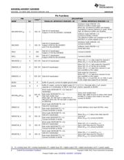
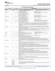
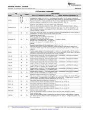
技术参数、封装参数在P7
应用领域在P1
电气规格在P8P9P10P11P12P13
导航目录
AD7656BSTZ数据手册
Page:
of 48 Go
若手册格式错乱,请下载阅览PDF原文件
SARADC
String
DAC
2.5V/3V
REF
BUSY/INT
RANGE/XCLK
HW/SW
REF /WR
RESET
EN
STBY
CS
RD
/
DB[15:0]
WORD/BYTE
PAR/SER
FS
CH_A0
CONVST_A
AGND
REFC_A
REF_IO
AVDD BVDD
BGND
AGND
HVDD HVSS
Control
Logic
Config
Register
I/O
SARADC
CH_A1
AGND
SARADC
CH_B0
CONVST_B
AGND
REFC_B
SARADC
CH_B1
AGND
SARADC
CH_C0
CONVST_C
AGND
REFC_C
SARADC
CH_C1
AGND
Clock
Generator
94
92
90
88
86
84
82
80
78
76
74
72
70
Signal-to-Noise Ratio (dB)
-40 -25 -10 5 20 35
50
65 125
Temperature (°C)
80 95 110
ADS8556
ADS8558
ADS8557
Product
Folder
Sample &
Buy
Technical
Documents
Tools &
Software
Support &
Community
An IMPORTANT NOTICE at the end of this data sheet addresses availability, warranty, changes, use in safety-critical applications,
intellectual property matters and other important disclaimers. PRODUCTION DATA.
ADS8556
,
ADS8557
,
ADS8558
SBAS404D –OCTOBER 2006–REVISED FEBRUARY 2016
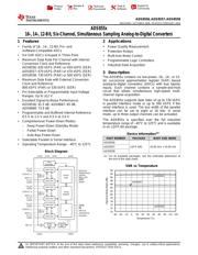
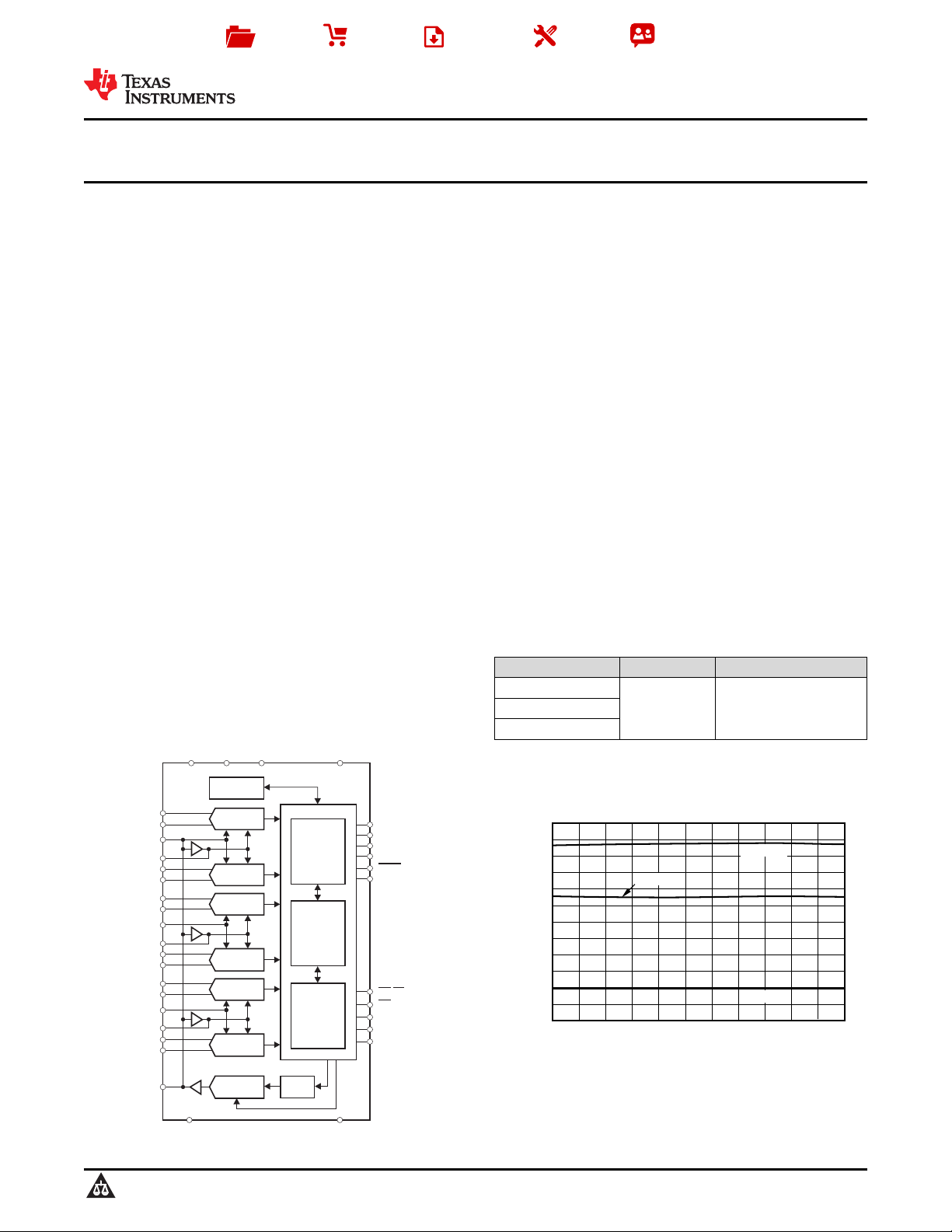
ADS855x
16-, 14-, 12-Bit, Six-Channel, Simultaneous Sampling Analog-to-Digital Converters
1
1 Features
1
• Family of 16-, 14-, 12-Bit, Pin- and
Software-Compatible ADCs
• Six SAR ADCs Grouped in Three Pairs
• Maximum Data Rate Per Channel with Internal
Conversion Clock and Reference:
ADS8556: 630 kSPS (PAR) or 450 kSPS (SER)
ADS8557: 670 kSPS (PAR) or 470 kSPS (SER)
ADS8558: 730 kSPS (PAR) or 500 kSPS (SER)
• Maximum Data Rate with External Conversion
Clock and Reference:
800 kSPS (PAR) or 530 kSPS (SER)
• Pin-Selectable or Programmable Input Voltage
Ranges: Up to ±12 V
• Excellent Signal-to-Noise Performance:
ADS8556: 91.5 dB, ADS8667: 85 dB,
ADS8668: 73.9 dB
• Programmable and Buffered Internal Reference:
0.5 V to 2.5 V and 0.5 V to 3.0 V
• Comprehensive Power-Down Modes:
– Deep Power-Down (Standby Mode)
– Partial Power-Down
– Auto-Nap Power-Down
• Selectable Parallel or Serial Interface
• Operating Temperature Range: –40°C to 125°C
Block Diagram
2 Applications
• Power Quality Measurement
• Protection Relays
• Multi-Axis Motor Control
• Programmable Logic Controllers
• Industrial Data Acquisition
3 Description
The ADS855x contains six low-power, 16-, 14-, or 12-
bit, successive approximation register (SAR) based
analog-to-digital converters (ADCs) with true bipolar
inputs. Each channel contains a sample-and-hold
circuit that allows simultaneous high-speed multi-
channel signal acquisition.
The ADS855x supports data rates of up to 730 kSPS
in parallel interface mode or up to 500 kSPS if the
serial interface is used. The bus width of the parallel
interface can be set to eight or 16 bits. In serial
mode, up to three output channels can be activated.
The ADS855x is specified over the full industrial
temperature range of –40°C to 125°C and is available
in an LQFP-64 package.
Device Information
(1)
PART NUMBER PACKAGE BODY SIZE (NOM)
ADS8556
LQFP (64) 10.00 mm × 10.00 mmADS8557
ADS8558
(1) For all available packages, see the orderable addendum at
the end of the data sheet.
SNR vs Temperature
器件 Datasheet 文档搜索
AiEMA 数据库涵盖高达 72,405,303 个元件的数据手册,每天更新 5,000 多个 PDF 文件
