Datasheet 搜索 > AD转换器 > ADI(亚德诺) > AD7709BRUZ 数据手册 > AD7709BRUZ 数据手册 5/32 页
 器件3D模型
¥ 32.265
AD7709BRUZ 数据手册 - ADI(亚德诺)
制造商:
ADI(亚德诺)
分类:
AD转换器
封装:
TSSOP-24
描述:
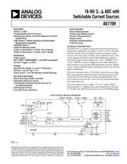
ANALOG DEVICES AD7709BRUZ 模数转换器, Σ-Δ, 16 bit, 2.7 V, 5.25 V, TSSOP
Pictures:
3D模型
符号图
焊盘图
引脚图
产品图
页面导航:

导航目录
AD7709BRUZ数据手册
Page:
of 32 Go
若手册格式错乱,请下载阅览PDF原文件

REV. A
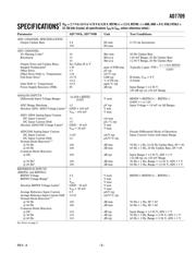
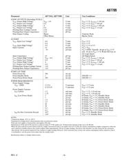
Parameter AD7709A,
AD7709
BUnit Test Conditions
LOGIC OUTPUTS (Excluding XTAL2)
V
OH
, Output High Voltage
2
V
DD
– 0.6 V min V
DD
= 3 V, I
SOURCE
= 100 mA
V
OL
, Output Low Voltage
2
0.4 V max V
DD
= 3 V, I
SINK
= 100 mA
V
OH
, Output High Voltage
2
4V min V
DD
= 5 V, I
SOURCE
= 200 mA
V
OL
, Output Low Voltage
2
0.4 V max V
DD
= 5 V, I
SINK
= 1.6 mA
Floating-State Leakage Current ± 10 mA max
Floating-State Output Capacitance ± 10 pF typ
Data Output Coding Binary Unipolar Mode
Offset Binary Bipolar Mode
I/O PORT
V
INL
, Input Low Voltage
2
0.8 V max V
DD
= 5 V
0.4 V max V
DD
= 3 V
V
INH
, Input High Voltage
2
2.0 V min V
DD
= 3 V or 5 V
Input Currents ± 2 mA max V
IN
= V
DD
–70 mA max V
IN
= GND, Typically –40 mA @ V
DD
= 5 V
and –20 mA at V
DD
= 3 V; Weak Pull-Ups on
the Logic Inputs
Input Capacitance 10 pF typ All Digital Inputs
V
OH
, Output High Voltage
2
V
DD
– 0.6 V min V
DD
= 3 V, I
SOURCE
= 100 mA
V
OL
, Output Low Voltage
2
0.4 V max V
DD
= 3 V, I
SINK
= 100 mA
V
OH
, Output High Voltage
2
4V min V
DD
= 5 V, I
SOURCE
= 200 mA
V
OL
, Output Low Voltage
2
0.4 V max V
DD
= 5 V, I
SINK
= 1.6 mA
Floating-State Output Leakage Current ± 10 mA max
Floating-State Output Capacitance ± 10 pF typ
START-UP TIME
From Power-On 300 ms typ
From Standby Mode 1 ms typ OSCPD = 0
From Power-Down Mode 300 ms typ OSCPD = 1
POWER REQUIREMENTS
Power Supply Voltage
V
DD
– GND 2.7/3.6 V min/max V
DD
= 3 V nom
4.75/5.25 V min/max V
DD
= 5 V nom
Power Supply Currents
I
DD
Current 1.5 mA max V
DD
= 3 V, 1.25 mA typ
1.75 mA max V
DD
= 5 V, 1.45 mA typ
I
DD
(Low Power Mode) 7 mA max B Grade, V
DD
= 3 V, Standby Mode
7 mA typ A Grade, V
DD
= 3 V, Standby Mode
1.5 mA max B Grade, V
DD
= 3 V, Power-Down Mode
1.5 mA typ A Grade, V
DD
= 3 V, Power-Down Mode
26 mA max B Grade, V
DD
= 5 V, Standby Mode
26 mA typ A Grade, V
DD
= 5 V, Standby Mode
6.5 mA max B Grade, V
DD
= 5 V, Power-Down Mode
6.5 mA typ A Grade, V
DD
= 5 V, Power-Down Mode
I
DD
for One Conversion Second 107
5
mA typ V
DD
= 3 V, Standby Mode
134
5
mA typ V
DD
= 5 V, Standby Mode
NOTES
1
Temperature Range –40∞C to +85∞C.
2
Guaranteed by design and/or characterization data on production release.
3
Full-scale error applies to both positive and negative full scale.
4
Simultaneous 50 Hz and 60 Hz rejection is achieved using 19.79 Hz update rate. Normal mode rejection in this case is 60 dB min.
5
When the part is placed in power-down mode for a single conversion/second, at an update rate of 19.79 Hz, the current consumption is higher compared to when the
part is placed in standby mode as the crystal oscillator takes approximately 100 ms to begin clocking. The device will, therefore, use full current for the conversion
time and the 100 ms period required for the oscillator to begin clocking. However, if the conversion rate is lower, the current consumption will be reduced so that it
is worthwhile to use the power-down rather than the standby mode.
Specifications subject to change without notice.
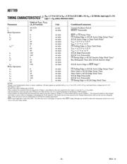
AD7709
–5–
器件 Datasheet 文档搜索
AiEMA 数据库涵盖高达 72,405,303 个元件的数据手册,每天更新 5,000 多个 PDF 文件
