Datasheet 搜索 > AD转换器 > ADI(亚德诺) > AD7891BP-1 数据手册 > AD7891BP-1 数据手册 3/20 页
 器件3D模型
¥ 40.189
AD7891BP-1 数据手册 - ADI(亚德诺)
制造商:
ADI(亚德诺)
分类:
AD转换器
封装:
PLCC-44
描述:
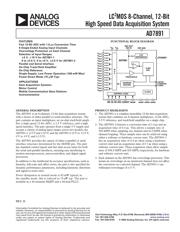
LC2MOS 8通道, 12位高速数据采集系统 LC2MOS 8-Channel, 12-Bit High Speed Data Acquisition System
Pictures:
3D模型
符号图
焊盘图
引脚图
产品图
页面导航:

导航目录
AD7891BP-1数据手册
Page:
of 20 Go
若手册格式错乱,请下载阅览PDF原文件

–3–
REV. D
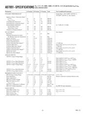
AD7891
Parameter A Version
1
B Version Y Version Unit Test Conditions/Comments
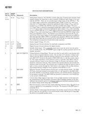
LOGIC OUTPUTS
Output High Voltage, V
OH
4.0 4.0 4.0 V min I
SOURCE
= 200 mA.
Output Low Voltage, V
OL
0.4 0.4 0.4 V max I
SINK
= 1.6 mA.
DB11to DB0
Floating-State Leakage Current ± 10 ± 10 ± 10 mA max
Floating-State Capacitance
5
15 15 15 pF max
Output Coding
Straight (Natural) Binary Data format bit of control register = 0.
Twos Complement Data format bit of control register = 1.
CONVERSION RATE
Conversion Time 1.6 1.6 1.6 ms max
Track/Hold Acquisition Time 0.6 0.6 0.6 ms max AD7891-1 hardware conversion.
0.7 0.7 0.7 ms max AD7891-1 software conversion.
0.4 0.4 0.4 ms max AD7891-2.
POWER REQUIREMENTS
V
DD
555V nom ± 5% for specified performance.
I
DD
Normal Mode 20 20 21 mA max
Standby Mode 80 80 80 mA max Logic inputs = 0 V or V
DD
.
Power Dissipation V
DD
= 5 V.
Normal Mode 100 100 105 mW max Typically 82 mW.
Standby Mode 400 400 400 mW max Typically 75 mW.
NOTES
1
Temperature ranges for the A and B Versions: –40∞C to +85∞C. Temperature range for the Y Version: –55∞C to +105∞C.
2
The AD7891-1’s dynamic performance (THD and SNR) and the AD7891-2’s THD are measured with an input frequency of 10 kHz. The AD7891-2’s SNR is
evaluated with an input frequency of 100 kHz.
3
This throughput rate can only be achieved when the part is operated in the parallel interface mode. Maximum achievable throughput rate in the serial interface mode
is 357 kSPS.
4
See the Terminology section.
5
Sample tested during initial release and after any redesign or process change that may affect this parameter.
6
REF IN must be buffered before being applied to V
INXB
.
Specifications subject to change without notice.
ABSOLUTE MAXIMUM RATINGS*
(T
A
= 25∞C, unless otherwise noted)
V
DD
to AGND . . . . . . . . . . . . . . . . . . . . . . . . . –0.3 V to +7 V
V
DD
to DGND . . . . . . . . . . . . . . . . . . . . . . . . . –0.3 V to +7 V
Analog Input Voltage to AGND
AD7891-1 . . . . . . . . . . . . . . . . . . . . . . . . . . . . . . . . . ± 17 V
AD7891-2 . . . . . . . . . . . . . . . . . . . . . . . . . . . . –5 V, +10 V
Reference Input Voltage to AGND . . . . –0.3 V to V
DD
+ 0.3 V
Digital Input Voltage to DGND . . . . . . –0.3 V to V
DD
+ 0.3 V
Digital Output Voltage to DGND . . . . . –0.3 V to V
DD
+ 0.3 V
Operating Temperature Range
Commercial (A, B Versions) . . . . . . . . . . . – 40∞C to +85∞C
Automotive (Y Version) . . . . . . . . . . . . . . –55∞C to +105∞C
Storage Temperature Range . . . . . . . . . . . . –65∞C to +150∞C
Junction Temperature . . . . . . . . . . . . . . . . . . . . . . . . . . 150∞C
MQFP Package, Power Dissipation . . . . . . . . . . . . . . 450 mW
q
JA
Thermal Impedance . . . . . . . . . . . . . . . . . . . . . . 95∞C/W
Lead Temperature, Soldering
Vapor Phase (60 sec) . . . . . . . . . . . . . . . . . . . . . . . . 215∞C
Infrared (15 sec) . . . . . . . . . . . . . . . . . . . . . . . . . . . 220∞C
PLCC Package, Power Dissipation . . . . . . . . . . . . . . 500 mW
q
JA
Thermal Impedance . . . . . . . . . . . . . . . . . . . . . . 55∞C/W
Lead Temperature, Soldering
Vapor Phase (60 sec) . . . . . . . . . . . . . . . . . . . . . . . . 215∞C
Infrared (15 sec) . . . . . . . . . . . . . . . . . . . . . . . . . . . 220∞C
*Stresses above those listed under Absolute Maximum Ratings may cause perma-
nent damage to the device. This is a stress rating only; functional operation of the
device at these or any other conditions above those listed in the operational
sections of this specification is not implied. Exposure to absolute maximum rating
conditions for extended periods may affect device reliability.
CAUTION
ESD (electrostatic discharge) sensitive device. Electrostatic charges as high as 4000 V readily
accumulate on the human body and test equipment and can discharge without detection.
Although the AD7891 features proprietary ESD protection circuitry, permanent damage may
occur on devices subjected to high energy electrostatic discharges. Therefore, proper ESD
precautions are recommended to avoid performance degradation or loss of functionality.
器件 Datasheet 文档搜索
AiEMA 数据库涵盖高达 72,405,303 个元件的数据手册,每天更新 5,000 多个 PDF 文件
