Datasheet 搜索 > DA转换器 > ADI(亚德诺) > AD7948BRSZ 数据手册 > AD7948BRSZ 数据手册 8/16 页
 器件3D模型
¥ 1.449
AD7948BRSZ 数据手册 - ADI(亚德诺)
制造商:
ADI(亚德诺)
分类:
DA转换器
封装:
SSOP-20
描述:
ANALOG DEVICES AD7948BRSZ 数模转换器, 12 bit, 17 MSPS, 串行, 3V 至 5.5V, 4.5V 至 5.5V, SSOP, 20 引脚
Pictures:
3D模型
符号图
焊盘图
引脚图
产品图
页面导航:
导航目录
AD7948BRSZ数据手册
Page:
of 16 Go
若手册格式错乱,请下载阅览PDF原文件
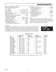
AD7943/AD7945/AD7948
REV. B–8–
TERMINOLOGY
Relative Accuracy
Relative Accuracy or endpoint linearity is a measure of the
maximum deviation from a straight line passing through the
endpoints of the DAC transfer function. It is measured after
adjusting for zero error and full-scale error and is normally
expressed in Least Significant Bits or as a percentage of full-
scale reading.
Differential Nonlinearity
Differential nonlinearity is the difference between the measured
change and the ideal 1 LSB change between any two adjacent
codes. A specified differential nonlinearity of 1 LSB maximum
ensures monotonicity.
Gain Error
Gain Error is a measure of the output error between an ideal
DAC and the actual device output. It is measured with all 1s
in the DAC after offset error has been adjusted out and is ex-
pressed in Least Significant Bits. Gain error is adjustable to
zero with an external potentiometer.
Output Leakage Current
Output leakage current is current which flows in the DAC lad-
der switches when these are turned off. For the I
OUT1
terminal,
it can be measured by loading all 0s to the DAC and measuring
the I
OUT1
current. Minimum current will flow in the I
OUT2
line
when the DAC is loaded with all 1s.
Output Capacitance
This is the capacitance from the I
OUT1
pin to AGND.
Output Voltage Settling Time
This is the amount of time it takes for the output to settle to a
specified level for a full-scale input change. For these devices, it
is specified both with the AD843 as the output op amp in the
normal current mode and with the AD820 in the biased current
mode.
Digital to Analog Glitch Impulse
This is the amount of charge injected into the analog output
when the inputs change state. It is specified as the area of the
glitch in nV-s. It is measured with the reference input connected
to AGND and the digital inputs toggled between all 1s and all
0s. As with Settling Time, it is specified with both the AD817
and the AD820.
AC Feedthrough Error
This is the error due to capacitive feedthrough from the DAC
reference input to the DAC I
OUT1
terminal, when all 0s are
loaded in the DAC.
Digital Feedthrough
When the device is not selected, high frequency logic activity on
the device digital inputs is capacitively coupled through the
device to show up as noise on the I
OUT1
pin and subsequently on
the op amp output. This noise is digital feedthrough.
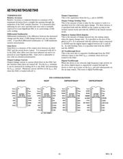
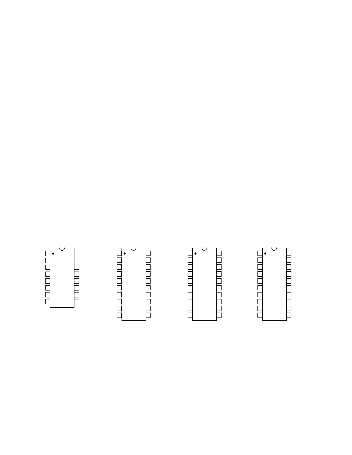
PIN CONFIGURATIONS
DIP/SOP SSOP DIP/SOP/SSOP DIP/SOP/SSOP
20
19
18
17
16
15
14
13
12
11
1
2
3
4
5
6
7
8
9
10
TOP VIEW
(Not to Scale)
AD7945
DB5
DB6
DB7
AGND
DGND
DB11
DB8
DB9
DB10
DB4
DB3
DB2
V
REF
V
DD
WR
DB1
DB0
CS
I
OUT1
R
FB
TOP VIEW
(Not to Scale)
AD7943
16
15
14
13
12
11
10
9
1
2
3
4
5
6
7
8
I
OUT1
I
OUT2
AGND
STB1
LD1
SRO
SRI
STB2
R
FB
V
REF
V
DD
CLR
DGND
STB4
STB3
LD2
TOP VIEW
(Not to Scale)
AD7943
20
19
18
17
16
15
14
13
12
11
1
2
3
4
5
6
7
8
9
10
NC = NO CONNECT
STB2
SRI
SRO
I
OUT2
AGND
STB1
LD1
NC
NC
LD2
STB3
STB4
V
REF
V
DD
CLR
DGND
NC
NC
I
OUT1
R
FB
TOP VIEW
(Not to Scale)
AD7948
20
19
18
17
16
15
14
13
12
11
1
2
3
4
5
6
7
8
9
10
DB4
DB5
DB6
AGND
DGND
CSMSB
DB7 (MSB)
CTRL
DF/DOR
DB3
DB2
DB1
V
REF
V
DD
WR
DB0 (LSB)
LDAC
CSLSB
I
OUT1
R
FB
器件 Datasheet 文档搜索
AiEMA 数据库涵盖高达 72,405,303 个元件的数据手册,每天更新 5,000 多个 PDF 文件
