Datasheet 搜索 > 放大器、缓冲器 > ADI(亚德诺) > AD8015ARZ-REEL7 数据手册 > AD8015ARZ-REEL7 数据手册 4/8 页

 器件3D模型
¥ 25.201
AD8015ARZ-REEL7 数据手册 - ADI(亚德诺)
制造商:
ADI(亚德诺)
分类:
放大器、缓冲器
封装:
SOIC-8
描述:
跨阻抗放大器 155Mbps Trnsimpdance
Pictures:
3D模型
符号图
焊盘图
引脚图
产品图
页面导航:
引脚图在P3Hot
原理图在P1P7
封装尺寸在P8
应用领域在P1P3

导航目录
AD8015ARZ-REEL7数据手册
Page:
of 8 Go
若手册格式错乱,请下载阅览PDF原文件
REV. A
–4–
AD8015
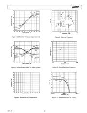
SONET OC-3 SENSITIVITY ANALYSIS
OC-3 Minimum Bandwidth = 0.7 × 155 MHz ≈ 110 MHz
Total Current Noise = (π/2) × 26.5 nA
= 42 nA (assuming single pole response)
To maintain a BER < 1 × 10
–10
(1 error per 10 billion bits):
Minimum current level needs to be > 13 × Total Current Noise
= 541 nA (peak)
Assume a typical photodiode current/power conversion ratio
= 0.85 A/W
Sensitivity (minimum power level) = 541/0.85 nW
= 637 nW (peak)
= –32.0 dBm (peak)
= –35.0 dBm (average)
The SONET OC-3 specification allows for a minimum power
level of –31 dBm peak, or –34 dBm average. Using the AD8015
provides 1 dB margin.
FDDI SENSITIVITY ANALYSIS
FDDI Minimum Bandwidth = 0.7 × 125 MHz ≈ 88 MHz
Total Current Noise = (π / 2) ×
88 MHz
100 MHz
× 26.5nA
= 39 nA (assuming single pole response)
To maintain a BER < 2.5 × 10
–10
(1 error per 4 billion bits):
Minimum current level needs to be > 12.6 × Total Current Noise
= 492 nA (peak)
Assume a typical photodiode current/power conversion ratio
= 0.85 A/W
Sensitivity (minimum power level) = 492/0.85 nW
= 579 nW (peak)
= –32.4 dBm (peak)
= –35.4 dBm (average)
The FDDI specification allows for a minimum power level of
–28 dBm peak, or –31 dBm average. Using the AD8015 pro-
vides 4.4 dB margin.
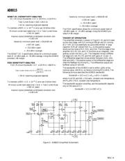
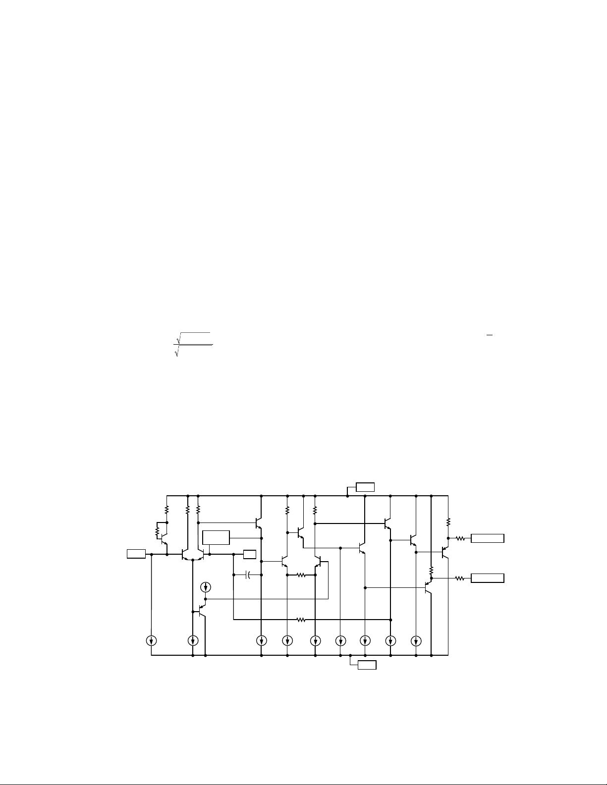
THEORY OF OPERATION
The simplified schematic is shown in Figure 5. Q1 and Q3 make
up the input stage, with Q3 running at 300 µA and Q1 running
at 2.7 mA. Q3 runs essentially as a grounded emitter. A large
capacitor (0.01 µF) placed from V
BYP
to the positive supply
shorts out the noise of R17, R21, and Q16. The first stage of the
amplifier (Q3, R2, Q4, and C1) functions as an integrator, inte-
grating current into the I
IN
pin. The integrator drives a differen-
tial stage (Q5, Q6, R5, R3, and R4) with gains of +3 and –3.
The differential stage then drives emitter followers (Q41, Q42,
Q60 and Q61). The positive output of the differential stage pro-
vides the feedback by driving R
FB
. The differential outputs are
buffered using Q7 and Q8.
The bandwidth of the AD8015 is set to within
+20% of the
nominal value, 240 MHz, by factory trimming R5 to 60 Ω. The
following formula describes the AD8015 bandwidth:
Bandwidth = 1/(2
π
× C1 × R
FB
× (R5 + 2 re)/R4)
where re (of Q5 and Q6) = 9 Ω each, constant over temperature,
and R
FB
/R4 = 43.5, constant over temperature.
The bandwidth equation simplifies, and the bandwidth depends
only on the value of C1:
Bandwidth = 1/(2
π
× 3393 × C1).
Q3
INPUT
CLAMPS
Q1
I
IN
Q16
R17
635
R1
300
R21
1.8k
V
BYP
R2
3k
+V
S
I10
0.75MA
C1 0.2pF
Q4
Q5
Q56
I1
1.5MA
I2
3MA
R5 60
R3
230
Q41
RFB
Q6
R4
230
Q7
+V
S
Q42
Q8
330
330
–V
S
+OUTPUT
R44 50
R43 50
I3
1MA
I4
3MA
I5
3MA
I6
1MA
I7
1MA
I8
1MA
I9
1MA
10k
Q61
Q60
–OUTPUT
Figure 5. AD8015 Simplified Schematiic
器件 Datasheet 文档搜索
AiEMA 数据库涵盖高达 72,405,303 个元件的数据手册,每天更新 5,000 多个 PDF 文件
