Datasheet 搜索 > 运算放大器 > ADI(亚德诺) > AD8040AR-REEL 数据手册 > AD8040AR-REEL 数据手册 17/20 页

 器件3D模型
¥ 0
AD8040AR-REEL 数据手册 - ADI(亚德诺)
制造商:
ADI(亚德诺)
分类:
运算放大器
封装:
SOIC
描述:
低功耗,高速轨到轨输入/输出放大器 Low Power, High Speed Rail-to-Rail Input/Output Amplifier
Pictures:
3D模型
符号图
焊盘图
引脚图
产品图
页面导航:
导航目录
AD8040AR-REEL数据手册
Page:
of 20 Go
若手册格式错乱,请下载阅览PDF原文件
AD8029/AD8030/AD8040
Rev. A | Page 17 of 20
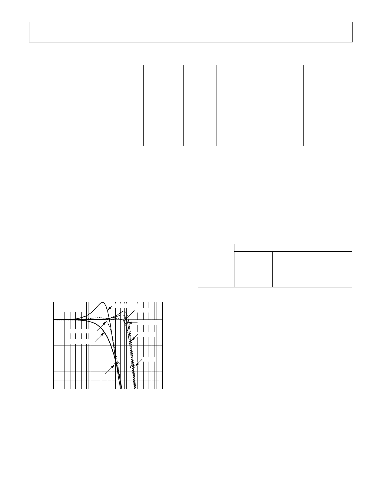
Table 5. Effect of Load on Performance
Noninverting
Gain
R
F
(kΩ)
R
G
(kΩ)
R
LOAD
(kΩ)
–3 dB SS BW
(MHz)
Peaking
(dB)
HD2 at 1 MHz,
2 V p-p (dB)
HD3 at 1 MHz,
2 V p-p (dB)
Output Noise
(nV/√Hz)
1 0 N/A 1 120 0.02 –80 –72 16.5
1 0 N/A 2 130 0.6 –84 –83 16.5
1 0 N/A 5 139 1 –87.5 –92.5 16.5
2 1 1 1 36 0 –72 –60 33.5
2 2.5 2.5 2.5 44.5 0.2 –79 –72.5 34.4
2 5 5 5 43 2 –84 –86 36
–1 1 1 1 40 0.01 –68 –57 33.6
–1 2.5 2.5 2.5 40 0.05 –74 –68 34
–1 5 5 5 34 1 –78 –80 36
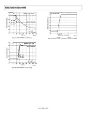
The feedback resistance (R
F
|| R
G
) combines with the input
capacitance to form a pole in the amplifier’s loop response. This
can cause peaking and ringing in the amplifier’s response if the
RC time constant is too low. Figure 55 illustrates this effect.
Peaking can be reduced by adding a small capacitor (1 pF–4 pF)
across the feedback resistor. The best way to find the optimal
value of capacitor is to empirically try it in your circuit. Another
factor of higher resistance values is the impact it has on noise
performance. Higher resistor values generate more noise. Each
application is unique and therefore a balance must be reached
between distortion, peaking, and noise performance. Table 5
outlines the trade-offs that different loads have on distortion,
peaking, and noise performance. In gains of 1, 2, and 10,
equivalent loads of 1 kΩ, 2 kΩ, and 5 kΩ are shown.
With increasing load resistance, the distortion and –3 dB
bandwidth improve, while the noise and peaking degrade
slightly.
R
L
= 5kΩ
FREQUENCY (MHz)
NORMALIZED CLOSED-LOOP GAIN (dB)
1
–8
10 100 1000
03679-A-007
2
1
0
–1
–2
–3
–4
–5
–6
R
L
= 2.5kΩ
–7
R
F
= R
L
= 5kΩ
R
F
= R
L
= 2.5kΩ
R
F
= R
L
= 1kΩ
G = +2
G = +1
R
L
= 1kΩ
V
S
= 5V
V
OUT
= 0.1V p-p
Figure 55. Frequency Response for Various Feedback/Load Resistances
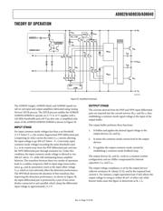
DISABLE PIN
The AD8029 disable pin allows the amplifier to be shut down
for power conservation or multiplexing applications. When in
the disable mode, the amplifier draws only 150 µA of quiescent
current. The disable pin control voltage is referenced to the
negative supply. The amplifier enters power-down mode any
time the disable pin is tied to the most negative supply or within
0.8 V of the negative supply. If left open, the amplifier will
operate normally. For switching levels, refer to Table 6.
Table 6. Disable Pin Control Voltage
Supply Voltage
Disable Pin
Voltage
+3 V +5 V
±5 V
Low
(Disabled) 0 V to <0.8 V 0 V to <0.8 V –5 V to <–4 .2 V
High
(Enabled) 1.2 V to 3 V 1.2 V to 5 V –3.8 V to +5 V
器件 Datasheet 文档搜索
AiEMA 数据库涵盖高达 72,405,303 个元件的数据手册,每天更新 5,000 多个 PDF 文件
