Datasheet 搜索 > 放大器、缓冲器 > ADI(亚德诺) > AD8210YRZ-REEL7 数据手册 > AD8210YRZ-REEL7 数据手册 1/16 页

 器件3D模型
¥ 44.193
AD8210YRZ-REEL7 数据手册 - ADI(亚德诺)
制造商:
ADI(亚德诺)
分类:
放大器、缓冲器
封装:
SOIC-8
描述:
高电压,双向电流分流监控器 High Voltage, Bidirectional Current Shunt Monitor
Pictures:
3D模型
符号图
焊盘图
引脚图
产品图
页面导航:
导航目录
AD8210YRZ-REEL7数据手册
Page:
of 16 Go
若手册格式错乱,请下载阅览PDF原文件
High Voltage, Bidirectional
Current Shunt Monitor
Data Sheet
AD8210
Rev. D Document Feedback
Information furnished by Analog Devices is believed to be accurate and reliable. However, no
responsibility is assumed by Analog Devices for its use, nor for any infringements of patents or other
rights of third parties that may result from its use. Specifications subject to change without notice. No
license is granted by implication or otherwise under any patent or patent rights of Analog Devices.
Trademarks and registered trademarks are the property of their respective owners.
One Technology Way, P.O. Box 9106, Norwood, MA 02062-9106, U.S.A.
Tel: 781.329.4700 ©2006–2013 Analog Devices, Inc. All rights reserved.
Technical Support www.analog.com
FEATURES
±4000 V HBM ESD
High common-mode voltage range
−2 V to +65 V operating
−5 V to +68 V survival
Buffered output voltage
5 mA output drive capability
Wide operating temperature range: −40°C to +125°C
Ratiometric half-scale output offset
Excellent ac and dc performance
1 μV/°C typical offset drift
10 ppm/°C typical gain drift
120 dB typical CMRR at dc
80 dB typical CMRR at 100 kHz
Available in 8-lead SOIC
Qualified for automotive applications
APPLICATIONS
Current sensing
Motor controls
Transmission controls
Diesel injection controls
Engine management
Suspension controls
Vehicle dynamic controls
DC-to-dc converters
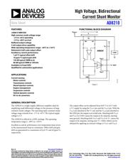
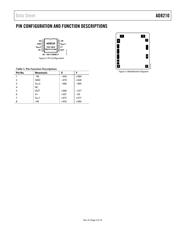
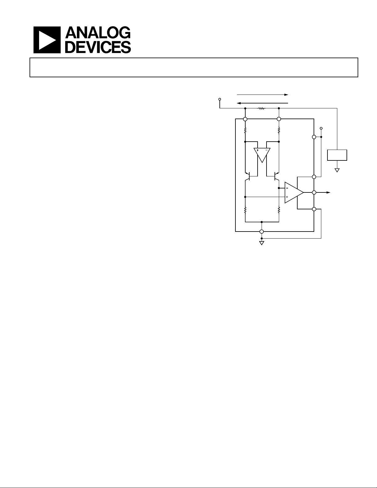
FUNCTIONAL BLOCK DIAGRAM
LOAD
AD8210
VOUT
G=+20
V
SUPPL Y
I
S
R
S
+IN –IN
V
S
V+
V
REF
1
V
REF
2
GND
05147-001
Figure 1.
GENERAL DESCRIPTION
The AD8210 is a single-supply, difference amplifier ideal for
amplifying small differential voltages in the presence of large
common-mode voltages. The operating input common-mode
voltage range extends from −2 V to +65 V. e typical supply
voltage is 5 V.
The AD8210 is offered in a SOIC package. The operating
temperature range is −40°C to +125°C.
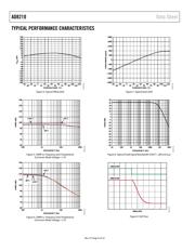
Excellent ac and dc performance over temperature keep errors
in the measurement loop to a minimum. Offset drift and gain
drift are guaranteed to a maximum of 8 μV/°C and 20 ppm/°C,
respectively.
The output offset can be adjusted from 0.05 V to 4.9 V with
a 5 V supply by using the V
REF
1 pin and the V
REF
2 pin. With the
V
REF
1 pin attached to the V+ pin and the V
REF
2 pin attached to
the GND pin, the output is set at half scale. Attaching both V
REF
1
and V
REF
2 to GND causes the output to be unipolar, starting
near ground. Attaching both V
REF
1 and V
REF
2 to V+ causes the
output to be unipolar, starting near V+. Other offsets can be
obtained by applying an external voltage to V
REF
1 and V
REF
2.
器件 Datasheet 文档搜索
AiEMA 数据库涵盖高达 72,405,303 个元件的数据手册,每天更新 5,000 多个 PDF 文件
